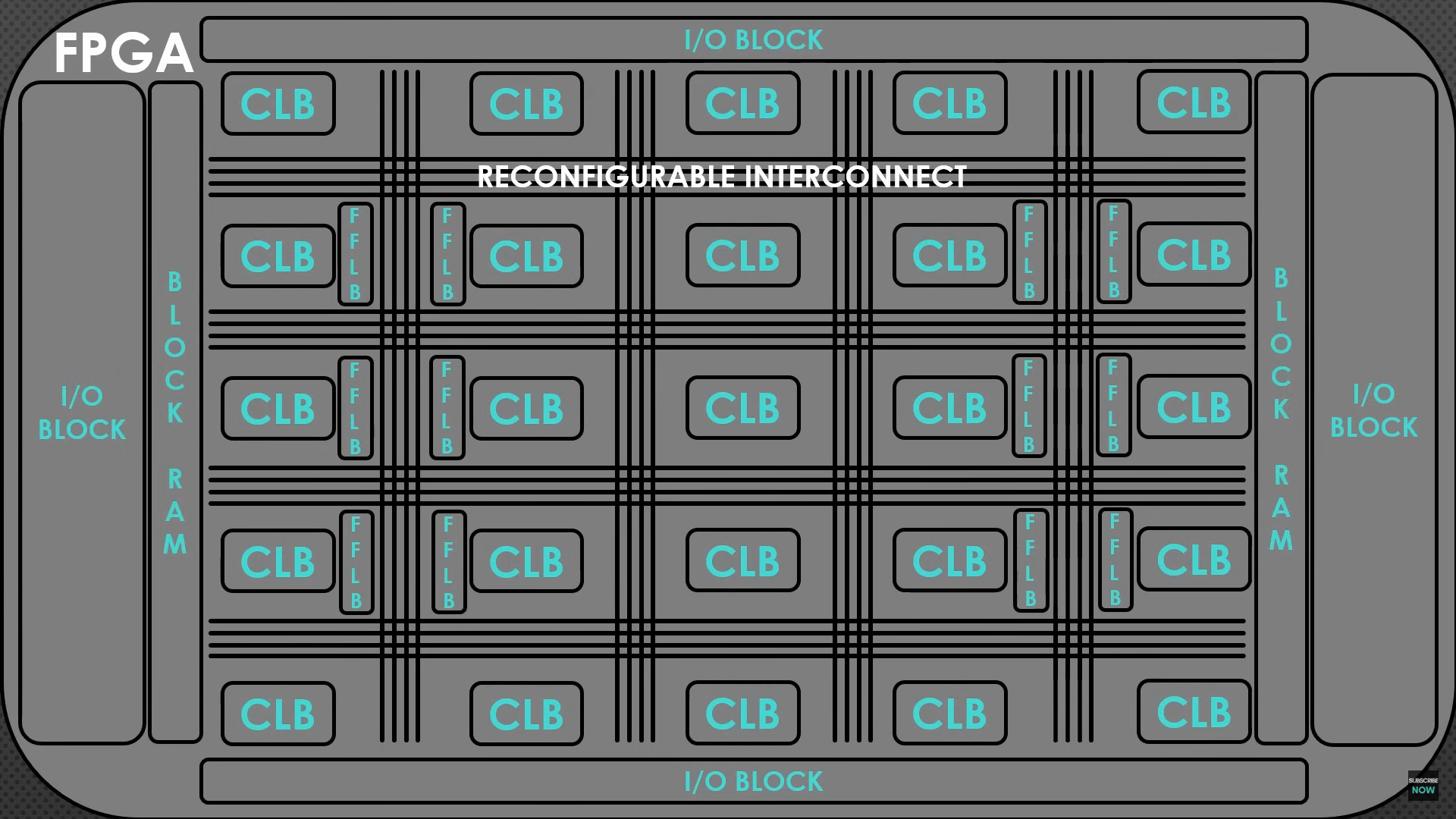
What is an FPGA?
A field-programmable gate array (FPGA) is a type of configurable integrated circuit that can be repeatedly programmed after manufacturing using hardware descriptive languages (Verilog in this blog).
This re-programmable nature distinguishes FPGAs from ASICs (Application specific integrated circuits).
FPGAs are made of a matrix of Configurable Logic Blocks (CLBs) with a mesh of reconfigurable interconnect which allows custom connection b/w different CLBs.
Advantages of FPGAs
- Faster : they can do parallel processing of signals
- Re-programming hardware structure : no money wasted on re-manufacturing board if any error occurs.
INFO
This blog is like a tutorial, we will be building small small projects while learning and gradually build up to bigger project, final being 8-bit counter on 7-segment display on our board.
1. Hello world : Switching LEDs
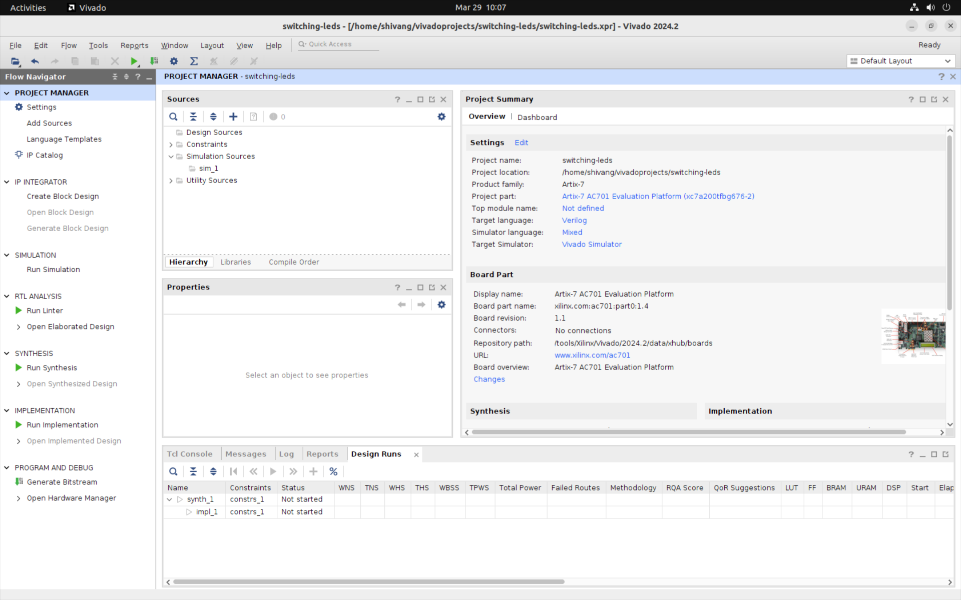
We do stuff in vivado : this is where we will be coding in verilog
Our verilog file = a source file for our project
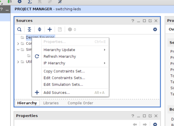
We will add design source
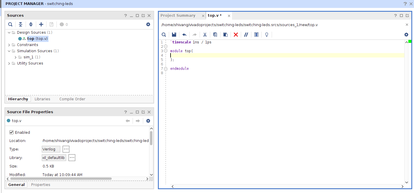
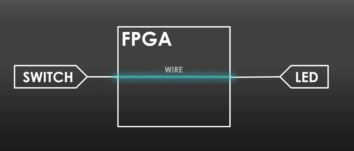
This is what we want to create
`timescale 1ns / 1ps

module top(
input switch,
output led
);

    assign led = switch; // If switch is turned on, LED is turned on asw

endmodule
We now also need to tell what pin is the switch and what pin is the LED on the FPGA.
We need to create a constraint file that will tell vivado where is the switch and where is the LED.
Add a constraint source under contraints folder
## LED
set_property -dict { PACKAGE_PIN _empty-space-left-rn_ IOSTANDARD LVCMOS33 } [get_ports {led}];

## SWITCH
set_property -dict { PACKAGE_PIN _empty-space-left-rn_ IOSTANDARD LVCMOS33 } [get_ports {switch}];
[get_ports {}] is the i/p and o/p from the verilog code we wrote, make sure the names are exactly the same
To know the PIN, we need the schematic of the board we are using, I will be using artix7
We can see on page 8 that SW0 is at pin R8 and the LED is at pin M26


## LED
set_property -dict { PACKAGE_PIN M26 IOSTANDARD LVCMOS33 } [get_ports {led}];

## SWITCH
set_property -dict { PACKAGE_PIN R8 IOSTANDARD LVCMOS33 } [get_ports {switch}];
Now we are done!
Now run synthesis, then run implementation, then generate bitstream from the left sidebar.
1. Synthesis
Purpose: The synthesis stage translates your high-level Verilog code (Register Transfer Level - RTL) into a lower-level netlist. This netlist is an abstract representation of the digital circuit using basic logic elements like flip-flops, logic gates (AND, OR, NOT, XOR), and memory blocks.
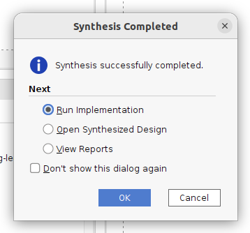
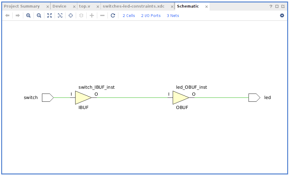
Let’s take a look at synthesized design first.
2. Run Implementation
Purpose: The implementation stage takes the synthesized netlist and maps it onto the physical resources of the target FPGA device. This involves deciding where each logic element will be placed on the chip and how they will be interconnected.
This will check if all timing requirements are met and that all FPGA pins are mapped correctly.
3. Generate Bitstream
Purpose: The bitstream generation stage takes the implemented design and translates it into a configuration file that can be downloaded onto the FPGA device to program its programmable fabric.
After it is completed, open Hardware Manager.
Make sure your board is connected to your computer, turn on the FPGA, then on the green callout in vivado on the top, click on open target and select auto connect.
We can now program the device by clicking program device on the same callout location. This will bring a popup to load the .bit bitstream file onto the FPGA and now we can control the LED!
2. Using the bus : 7 Segment Display
Design
Let’s start by creating a new project in vivado. This time, we use BlackBoard (xc7z007sclg400-1) FPGA since it has inbuilt 7 segment display.
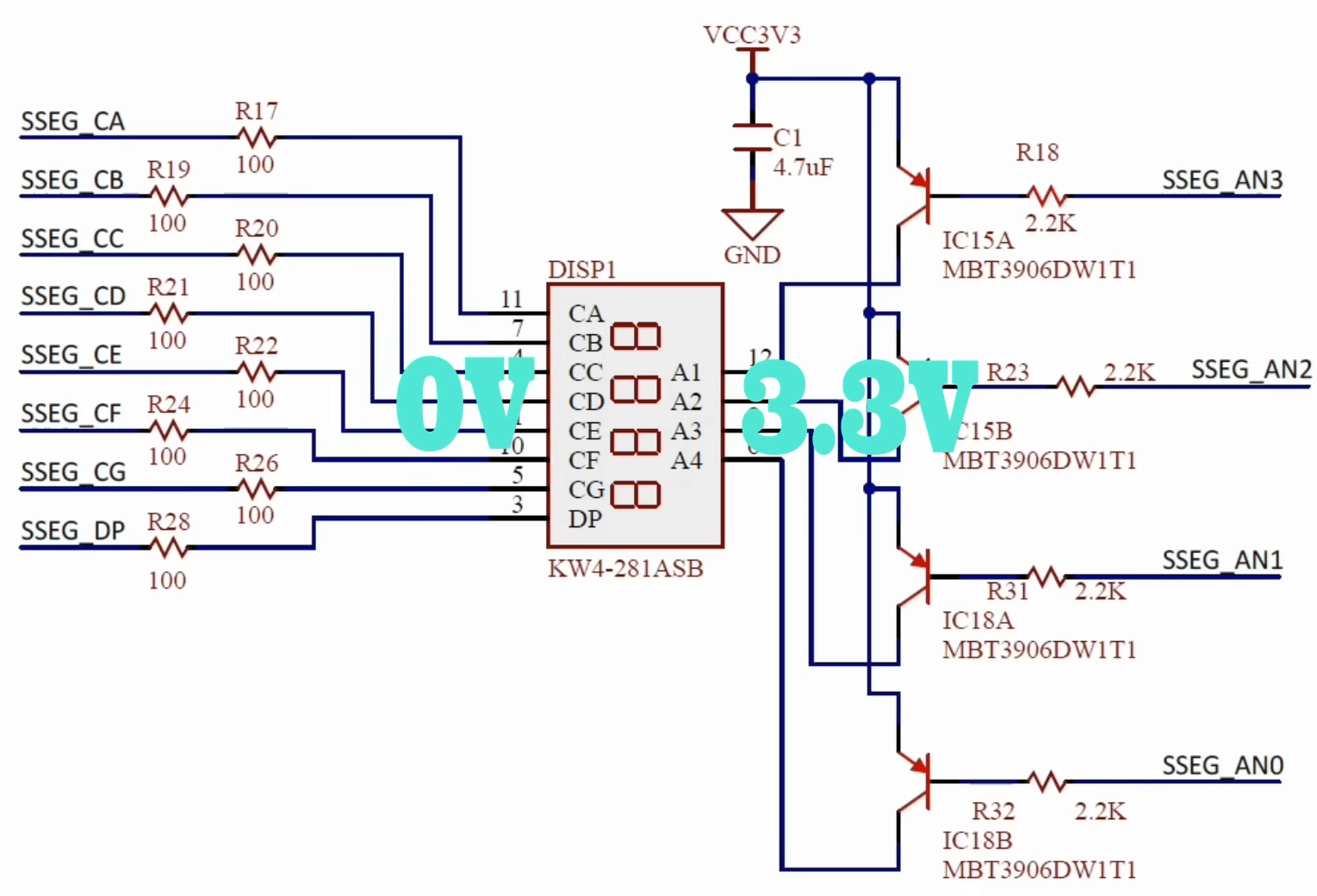
This is the schematic, we can see there are 8 FPGA pin connections on the left side, and 4 on the right.
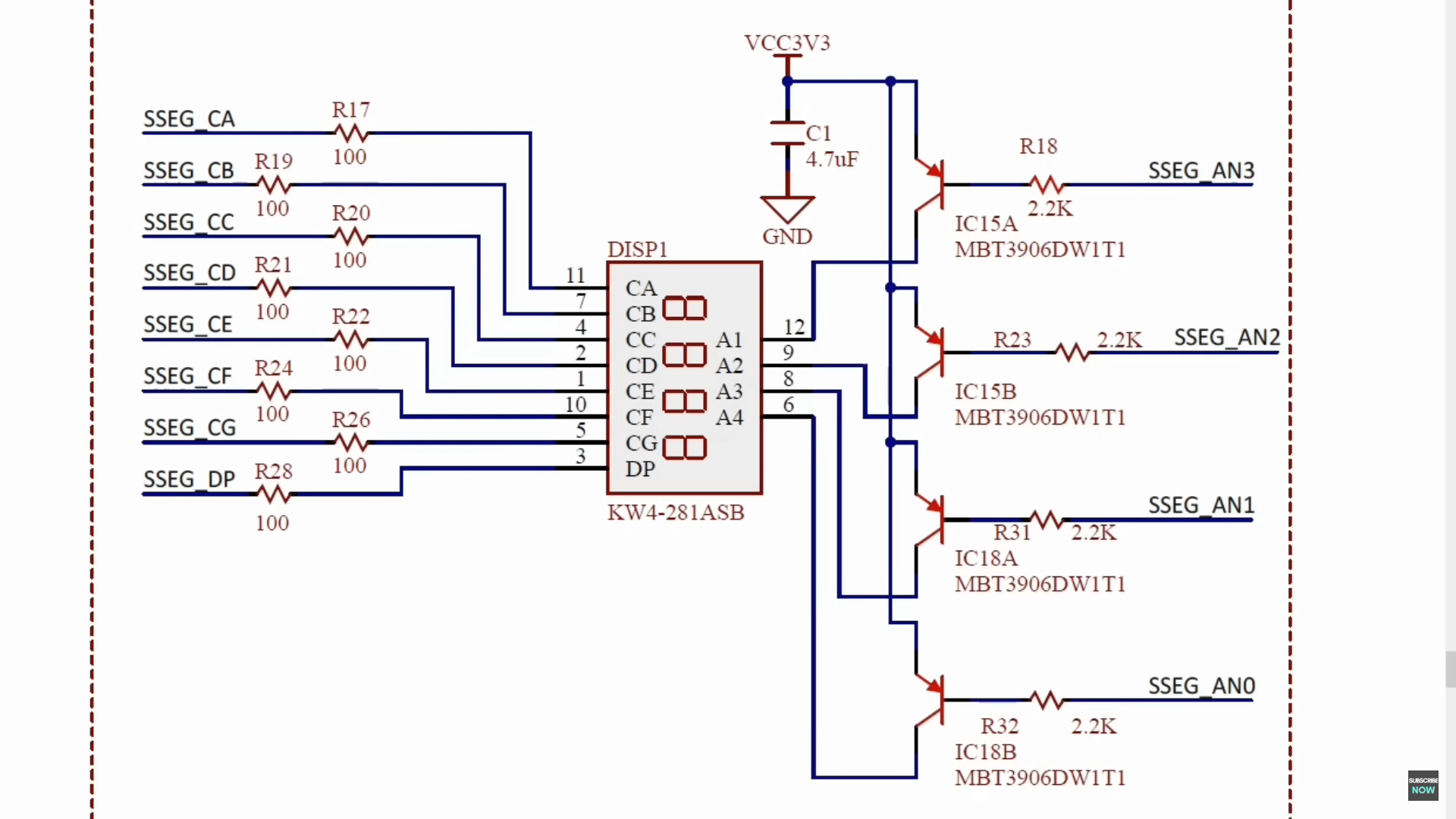
Each digit of the 7 segment display has 8 LEDs.
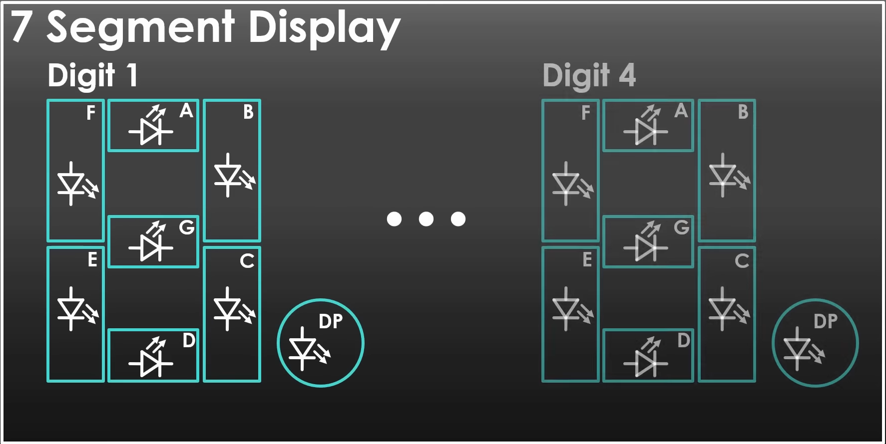
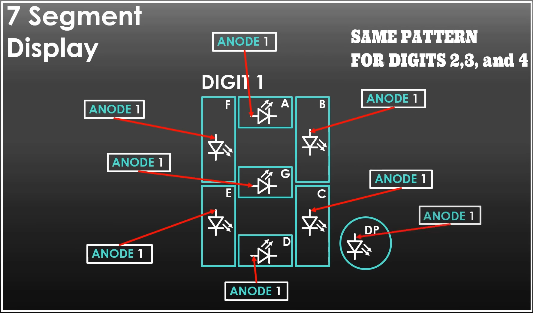
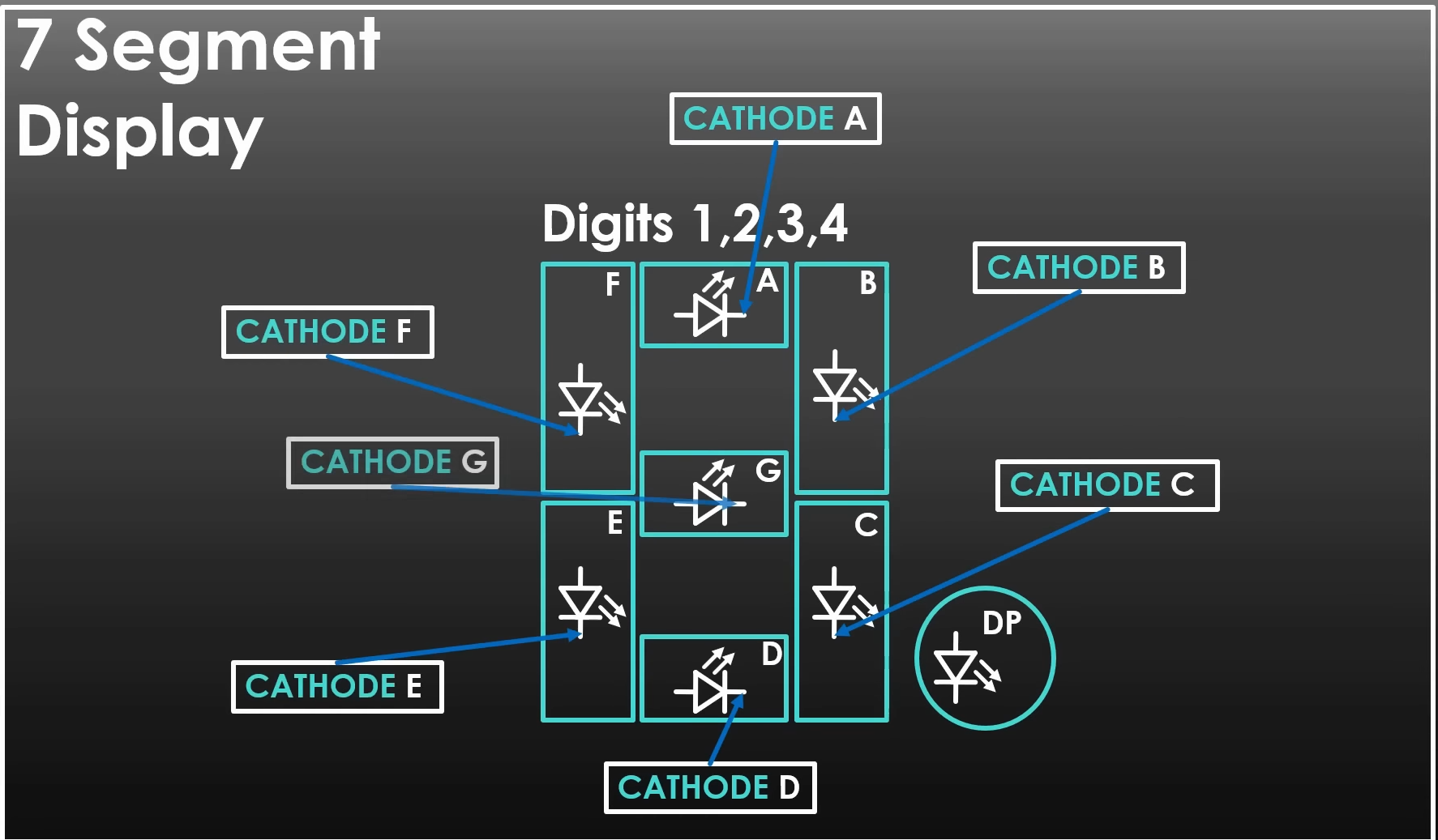
For each individual LED, one end is called the Anode, other, the Cathode.
| In the schemaic, connections on the left are cathodes, and the connections on the right are anodes. |  |
|---|---|
 |  |
In order to make an LED light up, we need to create voltage difference across anode and cathode. To achieve this, we will apply 0V on base of PNP transistors which will close the switch giving anode approximately 3.3V. And on the cathode side, we apply direct 0V.
Applying to code
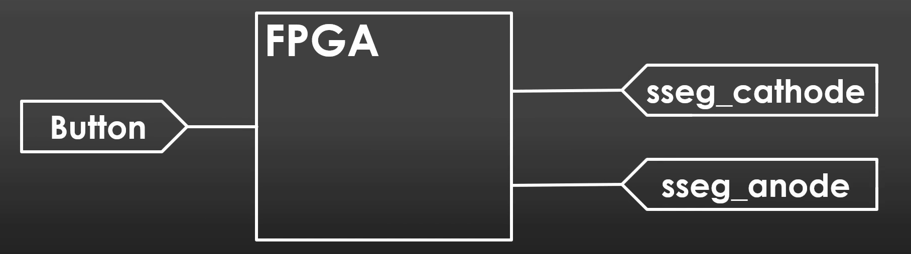
One input and 2 outputs.
`timescale 1ns / 1ps

module top(
input wire [3:0] button, // specifying wire is not necessary, its implicitly defined already.
output wire [7:0] sseg_cathode,
output wire [3:0] sseg_anode
);

    assign sseg_anode = button; // instead of sseg_anode[0] = button[0]; sseg_anode[1] = button[1]; ...
                                // means each wire in button bus is connected to same correspoinding number in anode bus
    assign sseg_cathode = 0;    // or sseg_cathode = 8'b00000000; or sseg_cathode = 8'd0; or sseg_cathode = 8'h00;

endmodule
[3:0] before button, [7:0] and [3:0 again are busses in verilog, its like an array which goes from 3(MSB) to 0(LSB) in binary. Its like an array, and it helps us avoid defining multiple wires separately.
There are 4 input buttons, 8 cathode outputs and 4 anode outputs.
Now the constraint file
#Push Buttons
set_property -dict { PACKAGE_PIN W14   IOSTANDARD LVCMOS33 } [get_ports { button[0] }]; #IO_L8P_T1_34 Schematic=BTN0
set_property -dict { PACKAGE_PIN W13   IOSTANDARD LVCMOS33 } [get_ports { button[1] }]; #IO_L4N_T0_34 Schematic=BTN1
set_property -dict { PACKAGE_PIN P15   IOSTANDARD LVCMOS33 } [get_ports { button[2] }]; #IO_L24P_T3_34 Schematic=BTN2
set_property -dict { PACKAGE_PIN M14   IOSTANDARD LVCMOS33 } [get_ports { button[3] }]; #IO_L23P_T3_35 Schematic=BTN3


#Seven Segmen Display Anodes
set_property -dict { PACKAGE_PIN K19   IOSTANDARD LVCMOS33 } [get_ports { sseg_anode[0] }]; #IO_L10P_T1_AD11P_35 Schematic=SSEG_AN0
set_property -dict { PACKAGE_PIN H17   IOSTANDARD LVCMOS33 } [get_ports { sseg_anode[1] }]; #IO_L13N_T2_MRCC_35 Schematic=SSEG_AN1
set_property -dict { PACKAGE_PIN M18   IOSTANDARD LVCMOS33 } [get_ports { sseg_anode[2] }]; #IO_L8N_T1_AD10N_35 Schematic=SSEG_AN2
set_property -dict { PACKAGE_PIN L16   IOSTANDARD LVCMOS33 } [get_ports { sseg_anode[3] }]; #IO_L11P_T1_SRCC_35 Schematic=SSEG_AN3

#Seven Segmen Display Cathodes
set_property -dict { PACKAGE_PIN K14   IOSTANDARD LVCMOS33 } [get_ports { sseg_cathode[0] }]; #IO_L20P_T3_AD6P_35 Schematic=SSEG_CA
set_property -dict { PACKAGE_PIN H15   IOSTANDARD LVCMOS33 } [get_ports { sseg_cathode[1] }]; #IO_L19P_T3_35 Schematic=SSEG_CB
set_property -dict { PACKAGE_PIN J18   IOSTANDARD LVCMOS33 } [get_ports { sseg_cathode[2] }]; #IO_L14P_T2_AD4P_SRCC_35 Schematic=SSEG_CC
set_property -dict { PACKAGE_PIN J15   IOSTANDARD LVCMOS33 } [get_ports { sseg_cathode[3] }]; #IO_25_35 Schematic=SSEG_CD
set_property -dict { PACKAGE_PIN M17   IOSTANDARD LVCMOS33 } [get_ports { sseg_cathode[4] }]; #IO_L8P_T1_AD10P_35 Schematic=SSEG_CE
set_property -dict { PACKAGE_PIN J16   IOSTANDARD LVCMOS33 } [get_ports { sseg_cathode[5] }]; #IO_L24N_T3_AD15N_35 Schematic=SSEG_CF
set_property -dict { PACKAGE_PIN H18   IOSTANDARD LVCMOS33 } [get_ports { sseg_cathode[6] }]; #IO_L8P_T1_AD10P_35 Schematic=SSEG_CG
set_property -dict { PACKAGE_PIN K18   IOSTANDARD LVCMOS33 } [get_ports { sseg_cathode[7] }]; #IO_L12N_T1_MRCC_35 Schematic=SSEG_DP
NOTE
You can get the XDC file by searching board name and finding its master.xdc online.
Now save the files and repeat the 3 step procedure showed in the switching LEDs example.
Pro tip : Or just click on generate bit-stream directly, it does all on it’s own.
3. Simulating code : Testbenches in verilog
We will create an RGB LED indicator and will use vivado simulator to test the code.
We wont be loading it on an FPGA board so doesn’t matter if your board has RBG LEDs or not.
First, let’s establish a plan for dividing the 16 inputs (represented by the 4-bit switch input) Here’s the truth table:
| switch[3:0] | Decimal | red | green | blue |
|---|---|---|---|---|
| 0000 | 0 | 1 | 0 | 0 |
| 0001 | 1 | 1 | 0 | 0 |
| 0010 | 2 | 1 | 0 | 0 |
| 0011 | 3 | 1 | 0 | 0 |
| 0100 | 4 | 0 | 1 | 0 |
| 0101 | 5 | 0 | 1 | 0 |
| 0110 | 6 | 0 | 1 | 0 |
| 0111 | 7 | 0 | 1 | 0 |
| 1000 | 8 | 0 | 0 | 1 |
| 1001 | 9 | 0 | 0 | 1 |
| 1010 | 10 | 0 | 0 | 1 |
| 1011 | 11 | 0 | 0 | 1 |
| 1100 | 12 | 0 | 0 | 1 |
| 1101 | 13 | 0 | 0 | 1 |
| 1110 | 14 | 0 | 0 | 1 |
| 1111 | 15 | 0 | 0 | 1 |
In a new vivado project, add this verilog design source.
`timescale 1ns / 1ps

module top(
    input [3:0] switch,
    output red,
    output green,
    output blue
);

    // Assign red when switch[3:2] = 00 (values 0-3)
    assign red = ~switch[3] & ~switch[2];
    // Assign green when switch[3:2] = 01 (values 4-7)
    assign green = ~switch[3] & switch[2];
    // Assign blue when switch[3] = 1 (values 8-15)
    assign blue = switch[3];


endmodule
To create a simulation file, right click Simulation Sources from the sources pane, and add simulation source.
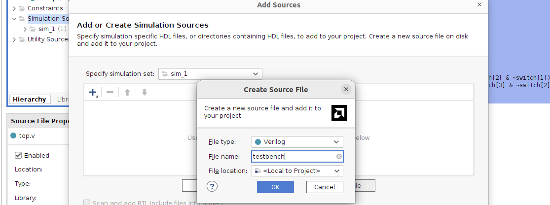
The testbench
`timescale 10ns / 1ps

module testbench();
// inputs, all inputs need to be a register, it retains it's values until a new value is assigned to it
reg [3:0] switch = 0; // you can only initialze registets not wires
// outputs, need to be wires
wire red;
wire green;
wire blue;

// Unit under test (UUT) : wrapper that ties the input and output of the verilog file we are simulating to the registers and wires of the testbench file.
top uut(
    .switch(switch), // .switch is from top module in verilog file, (switch) is from this simulation file
    .red(red),
    .green(green),
    .blue(blue)
);
integer k = 0;

initial
begin
    switch = 0;
    for(k=0; k<16; k=k+1)
    #10 switch = k; // Time delay (10 * 10ns) since timesacle is set is 1ns = 100ns

    #5 $finish;
end

endmodule
Now run simulation from the left sidebar, make sure you have gcc installed.
Notice the values of red, green and blue changing!
4. Clock : Blinking LED
We will be learning how clock works by creating a blinking LED using clock divider.
Clock input is really fast by default 100MHz (100 million cycles per second), the LED would be blinking soo fast we wouldn’t see it blinking.
We want to use a clock divider to divide down the clock signal.
Let’s also make our code modular now, we will create a seperate file for clocl_divider module.
1. clock_divider
`timescale 1ns / 1ps

// Counter based clock divider
module clock_divider(
    input wire clk,        // Input clock (100MHz = 10ns period, rising edge every 10ns)
    output reg divided_clk = 0  // Output clock (1Hz with current settings)
);
    // For 1Hz output (0.5s HIGH, 0.5s LOW):
    // div_value = 100MHz / ((2*desired freq) - 1) => 1Hz => 49999999
    // 100MHz input ÷ 49999999 = 2Hz, then toggle to get 1Hz
    // Each clock cycle = 10ns, so 49999999 cycles = 0.5s
    localparam div_value = 49999999;

    integer counter = 0;  // 32-bit wide counter

    // Counter logic
    // Triggers on each rising edge of the input clock (every 10ns)
    always@ (posedge clk)
    begin
        if (counter == div_value - 1)  // Use div_value-1 for exact timing
            counter <= 0;  // Reset counter when it reaches div_value-1
        else
            counter <= counter + 1;  // Increment counter
    end

    // Output clock generation
    // Toggles the output when counter reaches div_value-1
    always@ (posedge clk)
    begin
        if(counter == div_value - 1)
            divided_clk <= ~divided_clk;  // Flip output signal, Each count = 10ns, so 50M counts = 0.5s, divided_clk flips every 0.5s
        else
            divided_clk <= divided_clk;   // Maintain current output
    end

endmodule
2. Simulating the clock_divider
`timescale 1ns / 1ps
module testbench;
reg clk = 0; // 100MHz
wire divided_clk;
// Wrapper
clock_divider UUT(
.clk(clk),
.divided_clk(divided_clk)
);
always #5 clk = ~clk; // every 5 ns, signal flips => 10ns perios => 100MHz
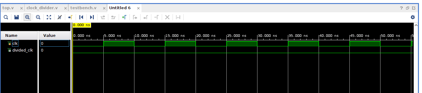
endmoduleIn vivado, by default running time is 1ns, this is too short since our divided clock will flip every 0.5s.
Change the simulation time to 1.1s atleast, it’ll take some time, have a cup of coffee.
Notice the divided clock flips every 0.5s
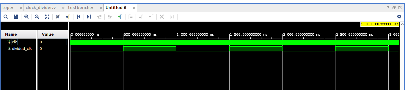 While the i/p clock flips every 5ns
3. Blinking LEDs
`timescale 1ns / 1ps

module top(
    input wire clk,
    output wire led
);

    // wrapper for the clock divider
    clock_divider wrapper(
        .clk(clk),
        .divided_clk(led)
    );
endmodule##Clock
set_property -dict { PACKAGE_PIN H16 IOSTANDARD LVCMOS33 } [get_ports { clk }];
#Individual LEDS
set_property -dict { PACKAGE_PIN N20 IOSTANDARD LVCMOS33 } [get_ports { led }]; #IO_L14P_T2_SRCC_34 Schematic=LD0Load the bit file on your board and the LED blinks!
5. Binary to BCD Decoder
Converting 8-bit binary to 8421 Binary coded decimal
The algorithm
The Double-Dabble Algorithm:
- Initialization: Start with all BCD digits set to zero.
- Iteration: For each bit in the binary number (from right to left):
- Shift: Shift the current BCD digits to the left (multiply by 2).
- Add Bit: Add the current bit of the binary number to the least significant BCD digit.
- Check and Add 3: If any BCD digit is 5 or greater, add 3 to that digit.
- Repeat: Continue these steps for all bits of the binary number.
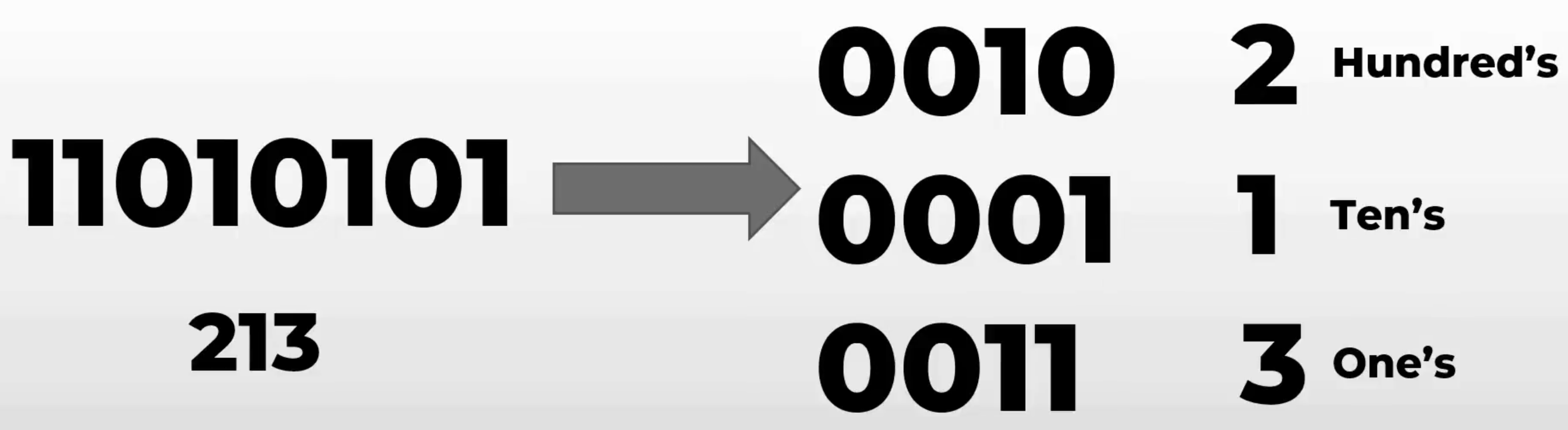
Example : 213 11010101
| Iteration | Current Bit | BCD Hundreds | BCD Tens | BCD Ones | Notes |
|---|---|---|---|---|---|
| Initial | - | 0000 | 0000 | 0000 | All BCD digits initialized to 0 |
| 1 | 1 (MSB) | 0000 | 0000 | 0001 | Shift BCD left, add MSB (1) |
| 2 | 1 | 0000 | 0000 | 0010 | Shift BCD left, add bit (1) |
| 0000 | 0000 | 0010 | No adjustment needed (all digits < 5) | ||
| 3 | 0 | 0000 | 0000 | 0100 | Shift BCD left, add bit (0) |
| 0000 | 0000 | 0100 | No adjustment needed (all digits < 5) | ||
| 4 | 1 | 0000 | 0000 | 1001 | Shift BCD left, add bit (1) |
| 0000 | 0001 | 0010 | Adjustment: ones digit > 4, add 3 → 1001 + 0011 = 1100, becomes 0001 0010 | ||
| 5 | 0 | 0000 | 0010 | 0100 | Shift BCD left, add bit (0) |
| 0000 | 0010 | 0100 | No adjustment needed (all digits < 5) | ||
| 6 | 1 | 0000 | 0100 | 1001 | Shift BCD left, add bit (1) |
| 0000 | 0101 | 0010 | Adjustment: ones digit > 4, add 3 → 1001 + 0011 = 1100, becomes 0101 0010 | ||
| 0000 | 1000 | 0010 | Adjustment: tens digit > 4, add 3 → 0101 + 0011 = 1000 | ||
| 7 | 0 | 0001 | 0000 | 0100 | Shift BCD left, add bit (0) |
| 0001 | 0000 | 0100 | No adjustment needed (all digits < 5) | ||
| 8 | 1 (LSB) | 0010 | 0000 | 1001 | Shift BCD left, add bit (1) |
| 0010 | 0001 | 0010 | Adjustment: ones digit > 4, add 3 → 1001 + 0011 = 1100, becomes 0001 0010 | ||
| Final | - | 0010 | 0001 | 0011 | Final BCD value: 213 |
The final BCD result is 0010 0001 0011, which represents 213 in decimal (2 hundreds, 1 ten, and 3 ones).
The 8-bit value 11010101 (213) was converted into BCD 0010 0001 0011 using this simple algorithm.
module bin2bcd(
    bin,
    bcd
    );
    //input ports and their sizes
    input [7:0] bin;
    //output ports and, their size
    output [11:0] bcd;
    //Internal variables
    reg [11 : 0] bcd;
     reg [3:0] i;

     //Always block - implement the Double Dabble algorithm
     always @(bin)
        begin
            bcd = 0; //initialize bcd to zero.
            for (i = 0; i < 8; i = i+1) //run for 8 iterations
            begin
                bcd = {bcd[10:0],bin[7-i]}; //concatenation

                //if a hex digit of 'bcd' is more than 4, add 3 to it.
                if(i < 7 && bcd[3:0] > 4)
                    bcd[3:0] = bcd[3:0] + 3;
                if(i < 7 && bcd[7:4] > 4)
                    bcd[7:4] = bcd[7:4] + 3;
                if(i < 7 && bcd[11:8] > 4)
                    bcd[11:8] = bcd[11:8] + 3;
            end
        end

endmodule`timescale 1ns / 1ps
module testbench;
// Input
reg [7:0] bin;
// Output
wire [11:0] bcd;
// Extra variables
reg [8:0] i;
// Instantiate the Unit Under Test (UUT)
bin2bcd uut (
.bin(bin),
.bcd(bcd)
);
//Simulation - Apply inputs
initial begin
//A for loop for checking all the input combinations.
for(i=0;i<256;i=i+1)
begin
bin = i;
#10; //wait for 10 ns.
end
$finish; //system function for stoping the simulation.
end
endmodule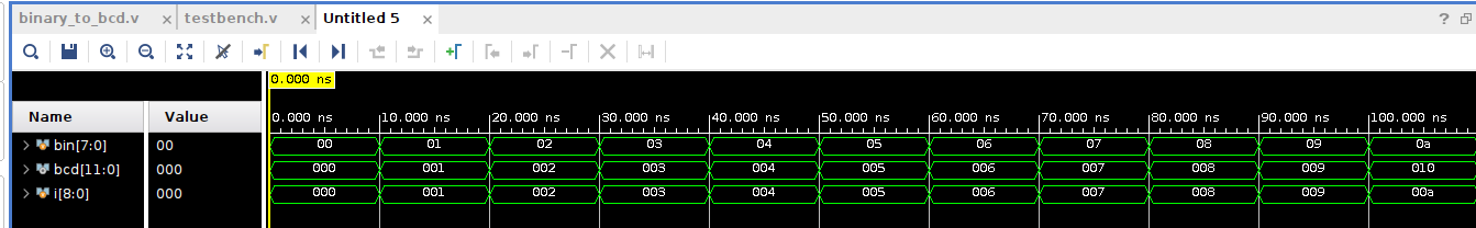
6. 8-bit counter
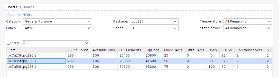
We will be using the Basys3 (Xilinx Artix-7 FPGA: XC7A35T-1CPG236C) board for this project.
Basys3 board schematic
Also refer to basys3-master.xdc
Transclude of basys3-master.xdc
Implementation
Create a new project with binary-to-bcd with this board
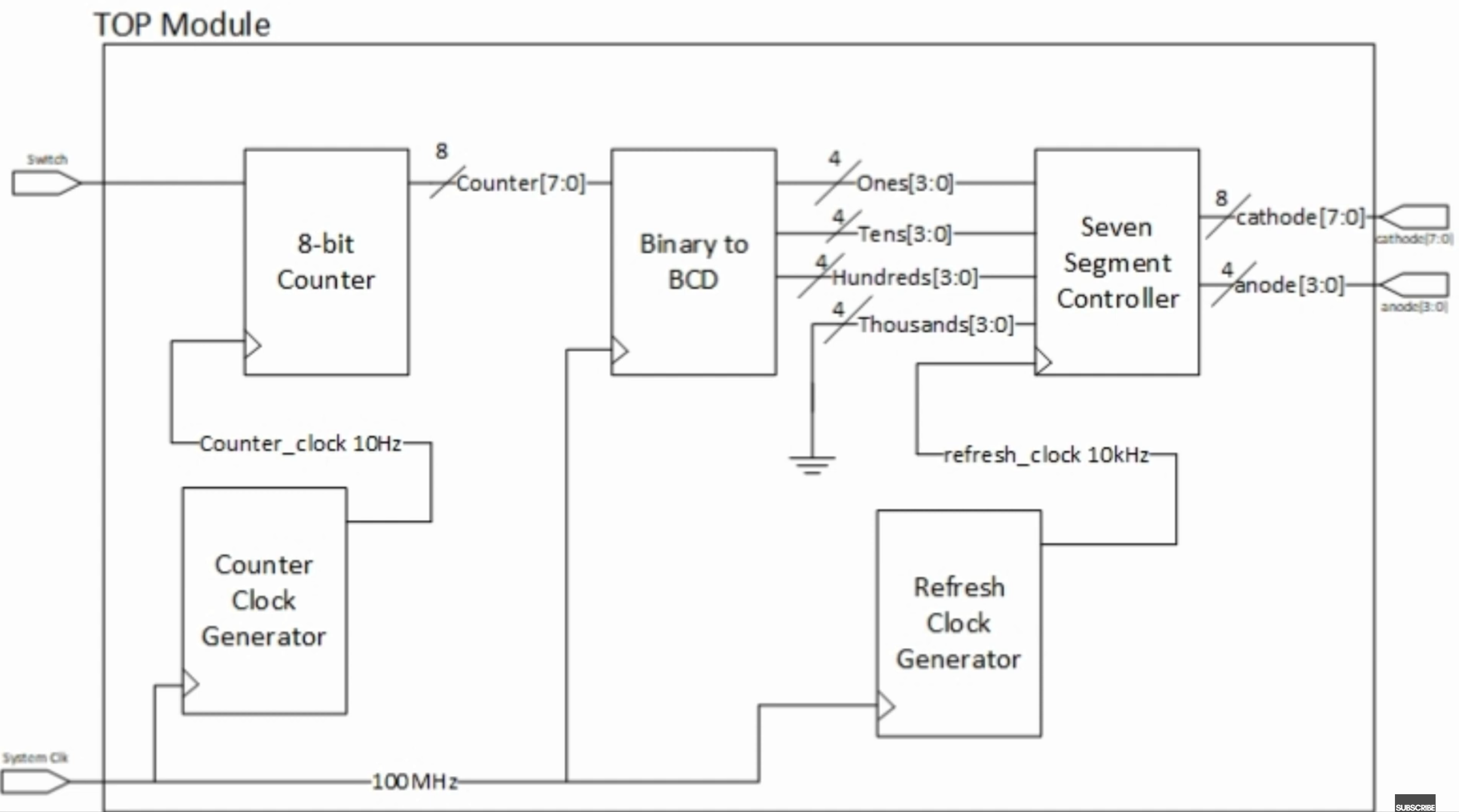
Files
Transclude of top.v
Transclude of 8_bit_counter.v
Transclude of counter_clock_gen.v
Transclude of refresh_clock_gen.v
Transclude of bin_to_bcd.v
Transclude of 7_seg_controller.v
Transclude of testbench.v
Transclude of basys3-8-bit-counter.xdc

Blog ends here
Below section is not related to FPGA or much to verilog
Logic Gates
Logic gates are devices that are used to implement boolean functions on one or more binary inputs and produces a single binary output.
Logic circuits (circuits made of multiple logic gates DUH) can be used to make devices like encoders, multiplexers, ALUs and even whole microprocessors!
We will go into a little bit more depth than required here at the transistor level.
NOTE
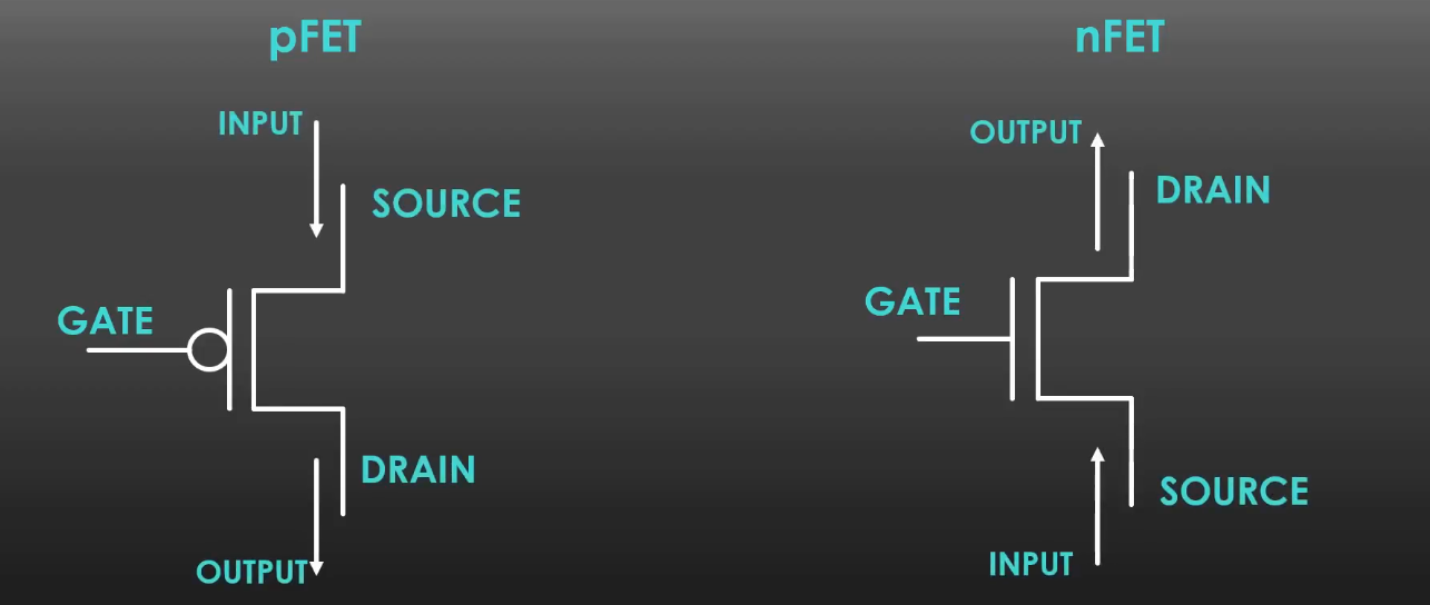
Logic gates are made of Feild effect transistors
pFETis like closed switch when logic 0 is applied at the Gate, andnFETis like closed switch when logic 1 is applied at the Gate.
pFETsused to pass through a logic 1 andnFETsused to pass through a logic 0.
1. Not
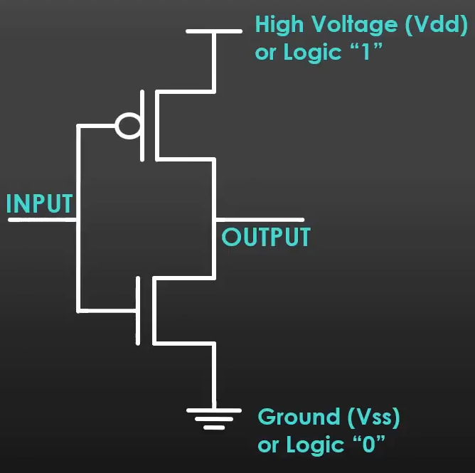
Try to simulate in your head what happens when you input a 0 or a 1, you know the output already, so go ahead and think.
I’ll help you out just in case : When i/p = 1, pFET is open, and nFET is closed ⇒ output is directly connected to ground, therefore, output = 0.
module not_gate(a,y);
input a;
output y;

assign y = ~a;

endmodule
2. And
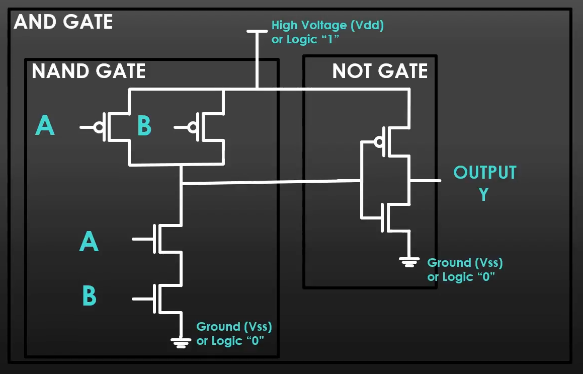
module and_gate(a,b,y);
input a,b;
output y;

assign y = a & b;

endmodule
3. Or
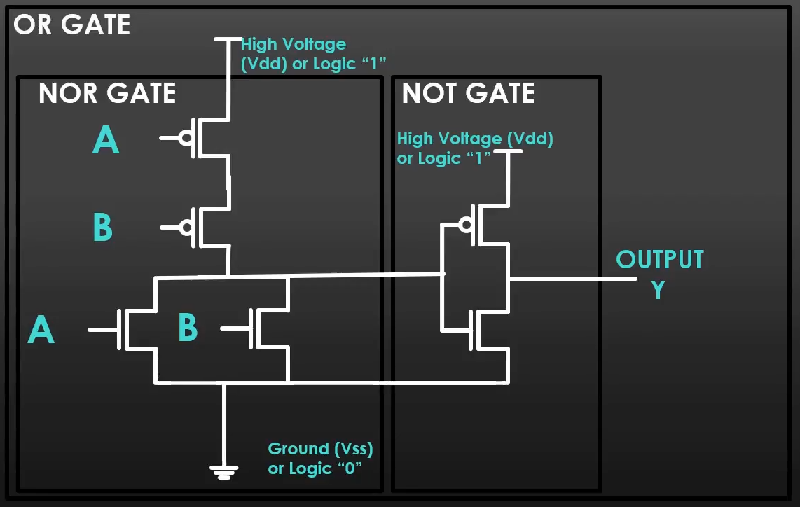
module or_gate(a,b,y);
input a,b;
output y;

assign y = a | b;

endmodule