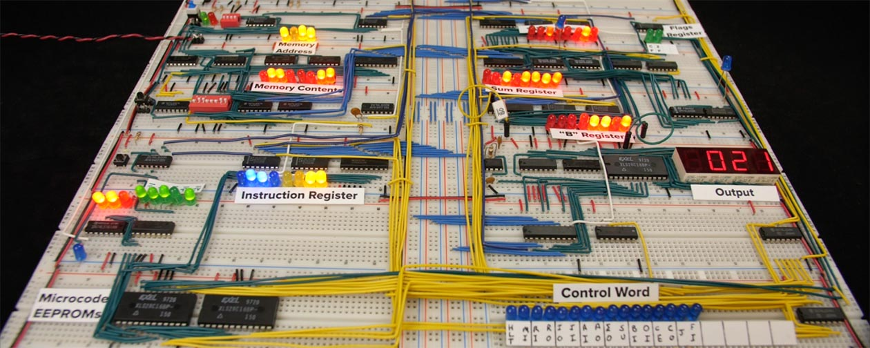
Final showcase
NOTE
To download all the final files, go to Here are all the final files
Why? My microprocessor and computer architecture teacher recently told in class that we could build a small toy processor on our own, I remember my eyes light up, cause?!?! it would be soo cool if I could build my own CPU and how much I would learn on the way…
We anyways had to do something for our semester final project, I asked one of my classmates if they wanted to do it and we set on the journey!
I began searching online on how to build a CPU from scratch when I came across Ben Eater’s 8-bit Breadboard Computer, but I read and realised that much of the fun was in the design and the learning, and the act of actually cutting wire was tedious exercise, and building from logic blocks would take too long!
Ben Eater’s 8-bit computer :
Background
After learning and documenting basics of how FPGA and verilog programming works in Intro to FPGA Programming, I want to recreate a CPU on an FPGA instead, it’s not tedious at all but still has just as much if not more learning!
Still getting inspiration from Ben Eater, he followed the design laid out in a book called Digital Computer Electronics by Malvino and Brown. The book builds what it calls the Simple-as-Possible (SAP) Computer. It starts with the incredibly simple SAP-1, adds some features to get the SAP-2, and then adds a few more to reach the final version called SAP-3.
For now, we will only be building SAP-1
SAP-1
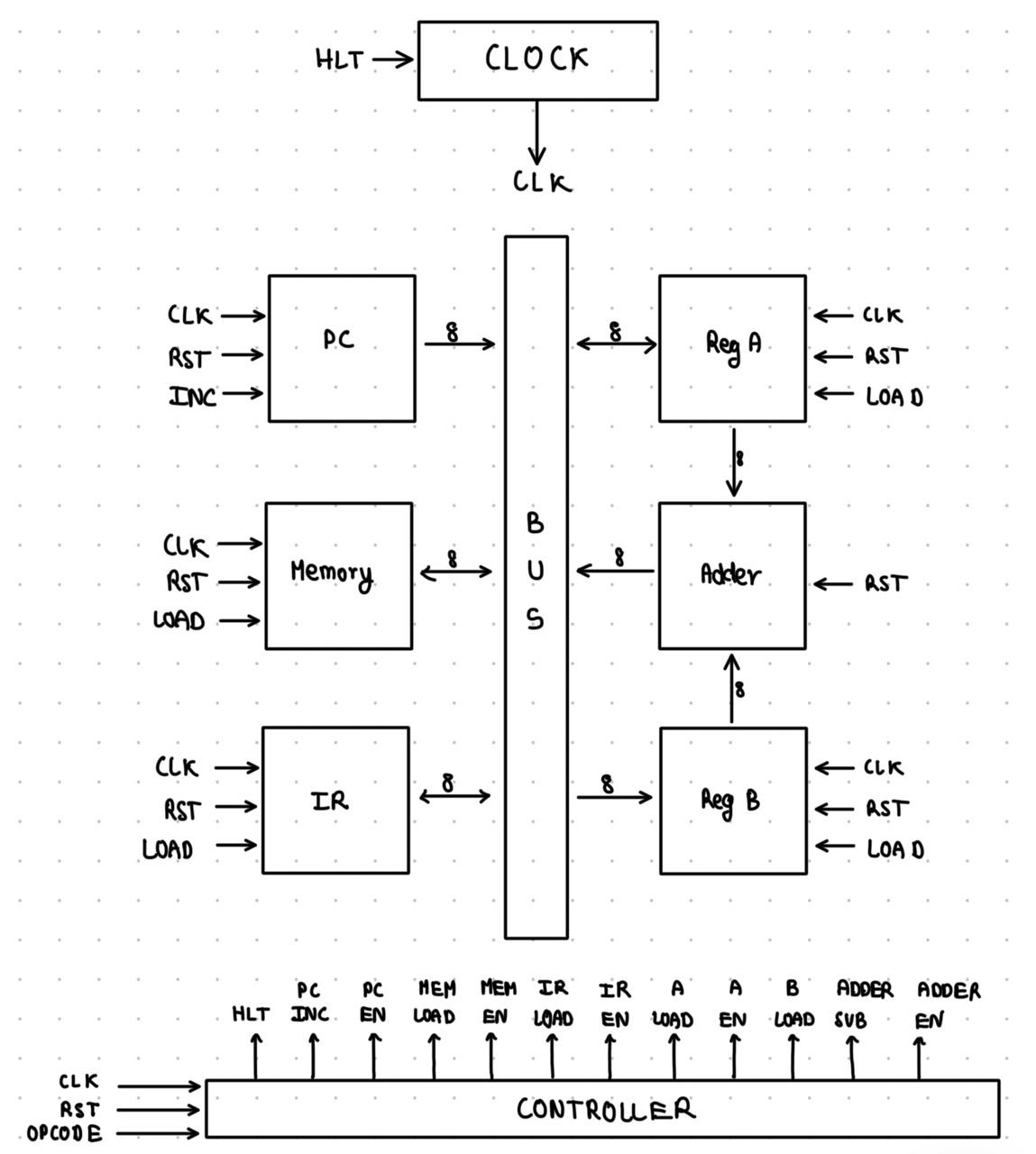
Modules
1. Clock
It orchestrates all of the distinct components so that they can talk together at a fixed interval in lock-step with each other. A clock oscillates between HIGH and LOW repeatedly, indefinitely.
// Clock module for Basys 3 with Halt functionality

module clock (
    input clk_100mhz, // Input from the Basys 3 100MHz oscillator (pin W5) [cite: 402]
    input hlt,        // Halt signal input
    output clk_out     // Clock output
);

    // Assign clk_out:
    // If hlt is asserted (1), output is 0.
    // Otherwise, output is the 100MHz clock input.
    assign clk_out = hlt ? 1'b0 : clk_100mhz;

endmodule
2. Program Counter
It always stores the address of the next instruction to be executed.
For the SAP-1, a program is just a series of bytes in memory where one byte makes up one instruction to be executed. The instructions are laid out serially and counted through starting from address 0.
The SAP-1’s memory is only 16 bytes so the program counter should count from 0x0 (0) to 0xF (15).
// Program Counter Module (4-bit for SAP-1)

module pc (
    input         clk, // Clock input
    input         rst, // Synchronous reset input
    input         inc, // Increment enable input
    output [3:0]  out  // 4-bit Program Counter output (addresses 0x0 to 0xF)
);

    // Internal register to store the 4-bit PC value
    reg [3:0] pc_reg;

    // Synchronous logic: updates happen on the positive edge of the clock
    always @(posedge clk) begin
        if (rst) begin
            // If reset is asserted, set PC to 0
            pc_reg <= 4'b0000;
        end else if (inc) begin
            // If increment is asserted (and not reset), increment PC by 1
            // It will automatically wrap from 15 (1111) back to 0 (0000)
            pc_reg <= pc_reg + 1;
        end
        // If neither rst nor inc is asserted, pc_reg retains its current value.
    end

    // Continuously assign the internal register value to the output port
    assign out = pc_reg;

endmodule
3. Register A
Register A is the main register of the computer and many of the instructions depend upon it. bus is an input which is driven by some other module and Register A can read from it when it needs to load which happens when load is asserted.
// Register A Module (8-bit)

module reg_a (
    input         clk,    // Clock input
    input         rst,    // Synchronous reset input
    input         load,   // Load enable input
    input  [7:0]  bus,    // 8-bit data input bus
    output [7:0]  out     // 8-bit data output
);

    // Internal register to store the value of Register A
    reg [7:0] reg_a_value;

    // Synchronous logic: updates happen on the positive edge of the clock
    always @(posedge clk) begin
        if (rst) begin
            // If reset is asserted, clear the register to 0
            reg_a_value <= 8'b00000000;
        end else if (load) begin
            // If load is asserted (and not reset),
            // capture the value from the bus into the register
            reg_a_value <= bus;
        end
        // If neither rst nor load is asserted, reg_a_value retains its current value.
    end

    // Continuously assign the internal register value to the output port
    assign out = reg_a_value;

endmodule
4. Register B
Register B is identical to Register A in design but when it’s used (as seen in the schematic diagram above), it never drives the bus directly; its output is fed to the Adder only.
The SAP-1 is designed so that Register A is where the main action occurs and Register B supports it.
// Register B Module (8-bit)

module reg_b (
    input         clk,    // Clock input
    input         rst,    // Synchronous reset input
    input         load,   // Load enable input
    input  [7:0]  bus,    // 8-bit data input bus
    output [7:0]  out     // 8-bit data output (intended for Adder)
);

    // Internal register to store the value of Register B
    reg [7:0] reg_b_value;

    // Synchronous logic: updates happen on the positive edge of the clock
    // Logic is identical to Register A
    always @(posedge clk) begin
        if (rst) begin
            // If reset is asserted, clear the register to 0
            reg_b_value <= 8'b00000000;
        end else if (load) begin
            // If load is asserted (and not reset),
            // capture the value from the bus into the register
            reg_b_value <= bus;
        end
        // If neither rst nor load is asserted, reg_b_value retains its current value.
    end

    // Continuously assign the internal register value to the output port
    assign out = reg_b_value;

endmodule
5. Adder
The SAP-1 can only do addition and subtraction. Don’t worry, it’ll be able to do much more soon!
The arithmetic module is called adder even tho it can perform both addition and subtraction (subtraction is just addition of a negative number after all).
// Adder/Subtractor Module (8-bit) for SAP-1

module adder (
    input  [7:0] in_a,      // 8-bit input from Register A
    input  [7:0] in_b,      // 8-bit input from Register B
    input        sub,       // Control signal: 0 = Add (A+B), 1 = Subtract (A-B)
    output [7:0] result     // 8-bit result of the operation
    // Note: Carry/Overflow flags are not explicitly generated as outputs
    // in the basic SAP-1 design, but could be added if needed.
);

    // This module is combinational. The output 'result' updates whenever
    // any of the inputs (in_a, in_b, subtract) change.

    // Use a continuous assignment with a ternary operator:
    // If 'subtract' is 1, perform subtraction (in_a - in_b).
    // If 'subtract' is 0, perform addition (in_a + in_b).
    assign result = sub ? (in_a - in_b) : (in_a + in_b);

endmodule
6. Memory
The Basys 3 board contains a 32Mbit non-volatile serial Flash device, which is attached to the Artix-7 FPGA using a dedicated quad-mode (x4) SPI bus. An Artix-7 35T configuration file requires just over two Mbytes of memory, leaving approximately 48% of the flash device available for user data.
The SAP-1 has 16 bytes of memory which is small enough that it can be defined directly inside of the FPGA.
There is a 4-bit register called the Memory Address Register (MAR) which is used to store a memory address. The SAP-1 takes two clock cycles to read from memory: one cycle loads an address from the bus into the MAR (using the load signal) and the second cycle uses the value in the MAR to address into ram and output that value onto the bus.
The initial block is used to initialize the memory by loading its contents from a file which is an easy way to set the memory. The file has sixteen lines where each line represents a byte of memory.
// SAP-1 Memory Module (16 Bytes with MAR)

module memory (
    input         clk,    // Clock input
    input         rst,    // Synchronous reset input
    input         load,   // Load enable for Memory Address Register (MAR)
    input  [7:0]  bus,    // Input bus (provides address for MAR on bits 3:0)
    output [7:0]  out     // Data output from RAM location pointed to by MAR
);

    // Declare the 16-byte x 8-bit RAM using registers
    // Addressable from 0 (0x0) to 15 (0xF)
    reg [7:0] ram [0:15];

    // Declare the 4-bit Memory Address Register (MAR)
    reg [3:0] mar;

    // Initialize memory content from an external file at power-up/simulation start
    // Create a file named "memory.hex" (or .bin) in your project directory.
    // It should contain 16 lines, each with an 8-bit hex (or binary) value.
    initial begin
        // Use $readmemh for a hex file (e.g., "memory.hex")
        // Use $readmemb for a binary file (e.g., "memory.bin")
        $readmemh("/home/shivang/vivadoprojects/8-bit-cpu/memory.hex", ram); ;

//        // For testing without a file, you can initialize manually:
//         ram[0] = 8'h01; // Example instruction LDA 15
//         ram[1] = 8'h0F;
//         ram[2] = 8'h11; // Example instruction ADD 14
//         ram[3] = 8'h0E;
//         // ... initialize other locations up to ram[15] ...
//         ram[14] = 8'h10; // Example data 16
//         ram[15] = 8'h20; // Example data 32
//         // Ensure all 16 locations are defined if using manual init
    end

    // MAR Logic: Load address bits from bus when 'load' is high
    always @(posedge clk) begin
        if (rst) begin
            // Reset MAR to 0 on reset
            mar <= 4'b0000;
        end else if (load) begin
            // Load the lower 4 bits from the bus into the MAR
            // Assuming address is placed on bus[3:0] during MAR load cycle
            mar <= bus[3:0];
        end
        // If neither rst nor load is high, MAR holds its previous value.
    end

    // Memory Read Logic: Combinational read based on current MAR value
    // The output 'out' always reflects the content of the RAM at the address stored in MAR.
    // The CPU controller determines when this 'out' value is actually driven onto the main bus.
    assign out = ram[mar];

endmodule
7. Instruction Register
The program counter contains the memory address to read the next instruction from, and the memory itself contains the instructions at that address, but there also needs to be a way to actually get the instruction from memory.
The instruction located at that memory address is retrieved from the main memory. This entire instruction (typically consisting of an opcode and an operand) is then loaded into the Instruction Register (IR).
The rst (reset) signal clears the IR, and the load signal enables the loading of a new instruction into it.
The complete instruction stored in the IR is available at the out output.
Subsequently, other parts of the processor will access the IR’s output and separate the instruction into its opcode (the operation to be performed, in the upper four bits) and the operand (the data or address the operation will act upon, in the lower four bits). If an instruction doesn’t require an operand, the lower four bits are simply disregarded.
// Instruction Register Module (8-bit) for SAP-1

module ir (
    input         clk,    // Clock input
    input         rst,    // Synchronous reset input
    input         load,   // Load enable input (captures instruction from bus)
    input  [7:0]  bus,    // 8-bit input bus (carrying the instruction byte)
    output [7:0]  out     // 8-bit output (the stored instruction byte)
);

    // Internal register to store the instruction
    reg [7:0] ir_value;

    // Synchronous logic: updates happen on the positive edge of the clock
    always @(posedge clk) begin
        if (rst) begin
            // If reset is asserted, clear the register to 0
            ir_value <= 8'b00000000;
        end else if (load) begin
            // If load is asserted (and not reset),
            // capture the instruction value from the bus into the register
            ir_value <= bus;
        end
        // If neither rst nor load is asserted, ir_value retains its current value.
    end

    // Continuously assign the internal register value (the full instruction)
    // to the output port 'out'. The controller logic will read this 'out'
    // signal and split it into opcode (out[7:4]) and operand (out[3:0]).
    assign out = ir_value;

endmodule
8. Bus
The bus serves as the central communication channel within the 8-bit computer, facilitating data exchange between all its constituent modules.
It comprises a set of eight parallel wires, dictated by the computer’s 8-bit architecture, ensuring that all data transfers occur in units of eight bits.
The process of sending and receiving data on the bus is meticulously coordinated through the use of specific control signals that are asserted (made active) at precise moments:
- A load signal instructs a receiving module to capture and store the data currently available on the bus.
- An enable signal activates a transmitting module, allowing its output to be placed onto the bus.
Ben Eater’s board vs FPGA : To select the proper module to be the only one driving the bus.
- Breadboard: Modules directly connect via chips with an enable pin. Only the enabled module drives the bus using high impedance (high-Z) for others.
- FPGA: Due to lack of internal high-Z, all module outputs (
out) are always active. A multiplexer, controlled by enable signals (adder_en,a_en,ir_en,mem_en,pc_en), selects only one module’s output to drive the bus. If no enable signal is active, the bus defaults to zero.
// System Bus Multiplexer Module for SAP-1

module bus_mux (
    // Data inputs from CPU components
    input [7:0] adder_out,    // Output from Adder/Subtractor
    input [7:0] a_out,        // Output from Register A
    input [7:0] ir_out,       // Output from Instruction Register (as requested)
    input [7:0] mem_out,      // Output from Memory
    input [3:0] pc_out,       // Output from Program Counter (4 bits)

    // Enable signals from Controller
    input       adder_en,     // Enable for Adder/Subtractor output
    input       a_en,         // Enable for Register A output
    input       ir_en,        // Enable for Instruction Register output (as requested)
    input       mem_en,       // Enable for Memory output
    input       pc_en,        // Enable for Program Counter output

    // Bus output - represents the value driven onto the bus
    output reg [7:0] bus_data // Use 'reg' because assigned in always block
);

    // Combinational logic block sensitive to changes in any input
    // Implements the multiplexer logic
    always @* begin
        // By default, drive zeros if no enable signal is active
        bus_data = 8'b00000000;

        if (adder_en) begin
            bus_data = adder_out;
        end else if (a_en) begin
            bus_data = a_out;
        end else if (ir_en) begin
            // As requested, place the full IR output on the bus when ir_en is high.
            // Note: In many SAP designs, only the operand part (ir_out[3:0]) might go here.
            bus_data = ir_out;
        end else if (mem_en) begin
            bus_data = mem_out;
        end else if (pc_en) begin
            // Zero-extend the 4-bit PC output to 8 bits for the bus
            bus_data = {4'b0000, pc_out};
        end
        // If none of the enable signals are high, bus_data remains the default value (zero).
    end

endmodule
9. Controller
The controller is the most complicated part of the computer and is where all of the interesting stuff happens. It decides what the computer will do next by asserting the different control signals that have gone into each of the modules.
Those control signals are:
| SIG | Description |
|---|---|
| hlt | Halt execution of the computer |
| pc_inc | Increment the Program Counter |
| pc_en | Put the value in the Program Counter onto the bus |
| mar_load | Load an address into the Memory Address Register |
| mem_en | Put a value from memory onto the bus |
| ir_load | Load a value from the bus into the Instruction Register |
| ir_en | Put the value in the Instruction Register onto the bus |
| a_load | Load a value from the bus into A |
| a_en | Put the value in A onto the bus |
| b_load | Load a value from the bus into B |
| adder_sub | Subtract the value in B from A |
| adder_en | Put the adder’s value onto the bus |
Instruction execution in the SAP-1 CPU proceeds in a fixed sequence of six stages, each lasting one clock cycle (Stage 0 to Stage 5, then repeating). A 3-bit stage register tracks the current stage, incrementing with each clock tick and resetting to 0 after Stage 5. Stage transitions occur on the negative clock edge to ensure control signals are ready for the next positive edge.
The opcode from the Instruction Register (IR) is sent to the controller. Based on the opcode and the current execution stage, the controller generates 12 control signals. These signals are bundled into a single 12-bit value for cleaner handling. Different instruction stages assert specific control signals to perform various operations.
The SAP-1 supports four instructions:
- LDA X (0000): Loads the value at memory address X into register A.
- ADD X (0001): Adds the value at memory address X to register A and stores the result in A.
- SUB X (0010): Subtracts the value at memory address X from register A and stores the result in A.
- HLT (1111): Stops program execution.
The first three stages are common to all instructions and handle instruction fetching:
- Stage 0: The Program Counter (PC)‘s value (the address of the next instruction) is placed on the bus, and this address is loaded into the Memory Address Register (MAR).
- Stage 1: The PC is incremented to point to the subsequent instruction in memory.
- Stage 2: The content of the memory location specified by the MAR is placed on the bus and loaded into the Instruction Register (IR).
The subsequent three stages (3-5) vary based on the specific instruction:
- LDA:
- Stage 3: The operand (memory address X) from the IR is placed on the bus and loaded into the MAR.
- Stage 4: The value from memory at address X (now in the MAR) is placed on the bus and loaded into register A.
- Stage 5: The CPU is idle.
- ADD:
- Stage 3: The operand (memory address X) from the IR is placed on the bus and loaded into the MAR.
- Stage 4: The value from memory at address X (now in the MAR) is placed on the bus and loaded into register B.
- Stage 5: The output of the adder (A + B) is placed on the bus and loaded into register A.
- SUB:
- Stage 3: The operand (memory address X) from the IR is placed on the bus and loaded into the MAR.
- Stage 4: The value from memory at address X (now in the MAR) is placed on the bus and loaded into register B.
- Stage 5: The adder is configured for subtraction (A - B), its output is placed on the bus, and loaded into register A.
- HLT:
- Stage 3: The system clock is halted, stopping further execution.
- Stage 4: The CPU is idle.
- Stage 5: The CPU is idle.
// SAP-1 CPU Controller Module (Updated Clock Edge)

module controller(
    input         clk,        // Clock input (This will be the *gated* clock from clock_halt)
    input         rst,        // Synchronous reset input
    input  [3:0]  opcode,     // Opcode from Instruction Register (IR[7:4])
    output [11:0] out         // 12-bit control word output
);

    // Control Signal Bit Mapping (same as before)
    localparam SIG_HLT       = 11;
    localparam SIG_PC_INC    = 10;
    localparam SIG_PC_EN     = 9;
    localparam SIG_MEM_LOAD  = 8; // MAR Load
    localparam SIG_MEM_EN    = 7;
    localparam SIG_IR_LOAD   = 6;
    localparam SIG_IR_EN     = 5;
    localparam SIG_A_LOAD    = 4;
    localparam SIG_A_EN      = 3;
    localparam SIG_B_LOAD    = 2;
    localparam SIG_ADDER_SUB = 1;
    localparam SIG_ADDER_EN  = 0;

    // Opcode Definitions (same as before)
    localparam OP_LDA = 4'b0000;
    localparam OP_ADD = 4'b0001;
    localparam OP_SUB = 4'b0010;
    localparam OP_HLT = 4'b1111;

    // Internal state registers
    reg [2:0]  stage;         // Execution stage (0-5)
    reg [11:0] ctrl_word;     // Intermediate register for control word
    reg        hlt_ff;        // Flip-flop to latch HALT state

    // --- Sequential Logic ---

    // Stage Counter (CHANGED to posedge clk)
    // Uses the gated clock 'clk' provided as input
    always @(posedge clk, posedge rst) begin // **** CHANGED TO POSEDGE ****
        if (rst) begin
            stage <= 3'b000;
        end else if (!hlt_ff) begin // Only advance if not halted
            if (stage == 3'd5) begin // Use decimal literal for clarity
                stage <= 3'b000;      // Wrap to Stage 0
            end else begin
                stage <= stage + 1;   // Go to next stage
            end
        end
        // else: stage register holds its value if halted
    end

    // Halt Flip-Flop: Set when HLT instruction reaches stage 3
    // Uses posedge clk (gated clock)
    always @(posedge clk or posedge rst) begin
        if (rst) begin
            hlt_ff <= 1'b0;
        // Set halt flip-flop only if HLT decoded at stage 3 and not already halted
        end else if (stage == 3'd3 && opcode == OP_HLT && !hlt_ff) begin
            hlt_ff <= 1'b1;
        end
        // else: halt flip-flop holds its value
    end

    // --- Combinational Logic ---

    // Generate the control word based on stage, opcode, and halt state
    // (Logic remains the same as your original version)
    always @(*) begin
        ctrl_word = 12'b000000000000; // Default: All inactive

        if (hlt_ff) begin
            ctrl_word[SIG_HLT] = 1'b1; // Only assert HLT if halted
        end else begin
            case (stage)
                3'd0: begin // Stage 0: PC -> MAR
                    ctrl_word[SIG_PC_EN]     = 1'b1;
                    ctrl_word[SIG_MEM_LOAD]  = 1'b1; // Assumed MAR Load
                end
                3'd1: begin // Stage 1: Increment PC
                    ctrl_word[SIG_PC_INC]    = 1'b1;
                end
                3'd2: begin // Stage 2: Memory -> IR
                    ctrl_word[SIG_MEM_EN]    = 1'b1;
                    ctrl_word[SIG_IR_LOAD]   = 1'b1;
                end
                3'd3: begin // Stage 3: Decode / Operand Address Fetch
                    case (opcode)
                        OP_LDA: begin ctrl_word[SIG_IR_EN] = 1'b1; ctrl_word[SIG_MEM_LOAD] = 1'b1; end
                        OP_ADD: begin ctrl_word[SIG_IR_EN] = 1'b1; ctrl_word[SIG_MEM_LOAD] = 1'b1; end
                        OP_SUB: begin ctrl_word[SIG_IR_EN] = 1'b1; ctrl_word[SIG_MEM_LOAD] = 1'b1; end
                        OP_HLT: begin ctrl_word[SIG_HLT] = 1'b1; end // HLT signal generated (latched next cycle)
                        default: ;
                    endcase
                end
                3'd4: begin // Stage 4: Data Fetch / Load B
                    case (opcode)
                        OP_LDA: begin ctrl_word[SIG_MEM_EN] = 1'b1; ctrl_word[SIG_A_LOAD] = 1'b1; end
                        OP_ADD: begin ctrl_word[SIG_MEM_EN] = 1'b1; ctrl_word[SIG_B_LOAD] = 1'b1; end
                        OP_SUB: begin ctrl_word[SIG_MEM_EN] = 1'b1; ctrl_word[SIG_B_LOAD] = 1'b1; end
                        default: ; // HLT is idle
                    endcase
                end
                3'd5: begin // Stage 5: Execution / Writeback A
                    case (opcode)
                        OP_ADD: begin ctrl_word[SIG_ADDER_EN] = 1'b1; ctrl_word[SIG_A_LOAD] = 1'b1; end
                        OP_SUB: begin ctrl_word[SIG_ADDER_SUB] = 1'b1; ctrl_word[SIG_ADDER_EN] = 1'b1; ctrl_word[SIG_A_LOAD] = 1'b1; end
                        default: ; // LDA, HLT are idle
                    endcase
                end
                default: ; // Should not happen
            endcase
        end // end if(!hlt_ff)
    end // end always @*

    // Final assignment
    assign out = ctrl_word;

endmodule
10. Combining all modules
The “top module” is the Verilog file that connects all the individual modules (pc, reg_a, reg_b, memory, ir, adder_subtractor, controller, bus_mux, clock_halt) together to form the complete CPU. It wires up the inputs and outputs of each component according to your design (and mirroring the connections in the testbench).
// SAP-1 CPU Top-Level Module with 7-Segment Display Output

module sap1_cpu_top (
    input         clk_in,     // Clock input (Connect to Basys 3 100MHz oscillator, e.g., W5)
    input         rst,        // Reset input (Connect to a button or reset circuit)
    output        hlt_out,    // Output the halt signal status (e.g., to an LED)

    // Outputs for the 7-Segment Display
    output [6:0]  seg_out,    // Segment cathodes (Active LOW)
    output [3:0]  an_out      // Anode selectors (Active HIGH)
);

    // --- Internal Signal Declarations ---

    // Clocks and Reset (as before)
    wire clk;       // Gated clock used by most components
    wire hlt;       // Internal halt signal from controller

    // Control Signals (as before)
    wire pc_inc;
    wire pc_en;
    wire mar_load;
    wire mem_en;
    wire ir_load;
    wire ir_en;
    wire a_load;
    wire a_en;
    wire b_load;
    wire adder_sub;
    wire adder_en;
    wire [11:0] control_word;

    // Data Paths & Intermediate Signals (as before)
    wire [7:0] bus_data;
    wire [3:0] pc_out_internal;
    wire [7:0] mem_out;
    wire [7:0] ir_out;
    wire [7:0] a_out; // <<< This holds the final result
    wire [7:0] b_out;
    wire [7:0] adder_out;
    wire [3:0] opcode;

    // --- Instantiate Clock Module --- (as before)
    clock u_clock (
        .clk_100mhz (clk_in),
        .hlt        (hlt),
        .clk_out    (clk)
    );

    // --- Instantiate CPU Components --- (as before)
    pc u_pc (.clk(clk), .rst(rst), .inc(pc_inc), .out(pc_out_internal));
    memory u_memory (.clk(clk), .rst(rst), .load(mar_load), .bus(bus_data), .out(mem_out));
    reg_a u_reg_a (.clk(clk), .rst(rst), .load(a_load), .bus(bus_data), .out(a_out));
    reg_b u_reg_b (.clk(clk), .rst(rst), .load(b_load), .bus(bus_data), .out(b_out));
    adder u_adder (.in_a(a_out), .in_b(b_out), .sub(adder_sub), .result(adder_out)); // Check '.sub' vs '.subt' if you used a different name
    ir u_ir (.clk(clk), .rst(rst), .load(ir_load), .bus(bus_data), .out(ir_out));

    // --- Instantiate Controller --- (as before)
    assign opcode = ir_out[7:4];
    controller u_controller (.clk(clk), .rst(rst), .opcode(opcode), .out(control_word));

    // --- Deconstruct Control Word --- (as before)
    assign hlt       = control_word[11];
    assign pc_inc    = control_word[10];
    assign pc_en     = control_word[9];
    assign mar_load  = control_word[8];
    assign mem_en    = control_word[7];
    assign ir_load   = control_word[6];
    assign ir_en     = control_word[5];
    assign a_load    = control_word[4];
    assign a_en      = control_word[3];
    assign b_load    = control_word[2];
    assign adder_sub = control_word[1];
    assign adder_en  = control_word[0];

    // --- Instantiate Bus Multiplexer --- (as before)
    bus_mux u_bus_mux (
        .adder_out(adder_out), .a_out(a_out), .ir_out(ir_out), .mem_out(mem_out), .pc_out(pc_out_internal),
        .adder_en(adder_en), .a_en(a_en), .ir_en(ir_en), .mem_en(mem_en), .pc_en(pc_en),
        .bus_data(bus_data)
    );

    // --- Instantiate Display Logic ---

    // 1. Convert final result (a_out) to BCD
    wire [3:0] bcd_h_w, bcd_t_w, bcd_o_w;
    binary_to_bcd u_bin_to_bcd (
        .bin_in       (a_out), // Input is the result from Register A
        .bcd_hundreds (bcd_h_w),
        .bcd_tens     (bcd_t_w),
        .bcd_ones     (bcd_o_w)
    );

    // 2. Instantiate the 7-Segment Controller
    seven_segment_controller u_display_controller (
        .clk      (clk_in), // Use the fast main clock for the controller's internal divider
        .reset    (rst),
        .enable   (hlt),    // Enable display only when CPU is halted
        .bcd_h    (bcd_h_w),
        .bcd_t    (bcd_t_w),
        .bcd_o    (bcd_o_w),
        .seg_out  (seg_out), // CORRECT: Connect to module's 'seg_out' port
        .an_out   (an_out)   // CORRECT: Connect to module's 'an_out' port
    );

    // --- Assign Top-Level Outputs ---
    assign hlt_out = hlt;

endmodule
11. Simulation
// Testbench for SAP-1 CPU Top-Level Module (sap1_cpu_top) with Detailed Logging
`timescale 1ns / 1ps

module top_tb();

    // --- Testbench Signals ---

    // Inputs to the DUT (sap1_cpu_top)
    reg  clk_in; // 100MHz clock input signal
    reg  rst;    // Reset signal

    // Outputs from the DUT (sap1_cpu_top)
    wire hlt_out;   // Halt status output
    wire [6:0] seg_out; // 7-Segment cathode outputs
    wire [3:0] an_out;  // 7-Segment anode selector outputs

    // --- Instantiate the Design Under Test (DUT) ---
    sap1_cpu_top u_dut (
        .clk_in(clk_in),
        .rst(rst),
        .hlt_out(hlt_out),
        .seg_out(seg_out),
        .an_out(an_out)
    );

    // --- Clock Generation ---
    parameter CLK_PERIOD = 10; // 10ns period for 100MHz
    initial begin
        clk_in = 0;
        forever #(CLK_PERIOD / 2) clk_in = ~clk_in;
    end

    // --- Reset Generation & Simulation Control ---
    initial begin
        // VCD Dump Setup
        $dumpfile("sap1_cpu_top_tb_detailed.vcd"); // New VCD filename
        $dumpvars(0, top_tb.u_dut); // Dump DUT internals

        // Reset Sequence
        $display("\n--- Simulation Start ---");
        rst = 1'b1; // Assert reset
        $display("@%t: Reset Asserted", $time);
        #(CLK_PERIOD * 2); // Hold reset
        rst = 1'b0; // De-assert reset
        $display("@%t: Reset De-asserted", $time);

        // Simulation Duration
        #6000; // Increased duration slightly for more post-halt observation

        $display("\n--- Simulation Finished @ Time %t ns ---", $time);
        $finish;
    end
endmodule
Feeding instructions
Right now in our memory.v file, we are hard-coding instructions.
Instead now, we will go through how to convert our assembly code into a .hex file and feed it to our memory.v.
Since your SAP-1 CPU has a custom instruction set, we can’t use standard assemblers like the ARM one. We need to define our own simple assembly format and create a script to “assemble” it directly into the hex format needed by your memory.v’s $readmemh.
1. Define the SAP-1 Assembly Language
Let’s use simple mnemonics. Remember:
- Instructions are 8 bits:
Opcode (4 bits) | Operand (4 bits) - Operand for LDA/ADD/SUB is a memory address (0-F).
- Operand for HLT is ignored (conventionally 0).
We’ll create a file, say program.sap1, with this content:
# --- My SAP-1 Test Program ---
# Goal: Compute 10 + 20 - 10 = 20 (0x14)

# Code Section
LDA E   # Load value from address 0xE (should be 10 = 0x0A) into Reg A
ADD F   # Add value from address 0xF (should be 20 = 0x14) to Reg A. A = 0x0A + 0x14 = 0x1E
SUB E   # Subtract value from address 0xE (0x0A) from Reg A. A = 0x1E - 0x0A = 0x14
HLT     # Halt execution

# Padding directives to place data correctly
# Ensure next data byte is at address 0xE
.PAD E

# Data Section
.BYTE 0A # Define byte at address 0xE (Value = 10)
.BYTE 14 # Define byte at address 0xF (Value = 20)

# --- End of Program ---
Key Elements:
LDA,ADD,SUB: Instructions followed by a single hex digit address (0-F).HLT: Instruction, no operand needed..PAD <hex_address>: A directive telling our assembler script to fill memory with00until the specified address is reached..BYTE <hex_byte>: A directive to place a specific 8-bit hex value at the current memory address.#: Comments, ignored by the script.
2. Create the Bash “Assembler” Script (assemble_sap1.sh)
This script will read program.sap1, parse it, and generate memory.hex.
#!/bin/bash

# --- Simple SAP-1 Assembler Script ---

# Input assembly file is the first argument
input_asm_file="$1"
# Output hex file for Verilog memory initialization
output_hex_file="memory.hex"
# Total memory size for SAP-1 (16 bytes)
mem_size=16

# --- Input Validation ---
if [[ -z "$input_asm_file" ]]; then
  echo "Usage: $0 <input_assembly_file.sap1>"
  exit 1
fi

if [[ ! -f "$input_asm_file" ]]; then
  echo "Error: Input file '$input_asm_file' not found."
  exit 1
fi

# --- Opcode Definitions (4-bit Hex Nibbles) ---
# Associative array to map instruction mnemonics to hex opcodes
declare -A opcodes=(
  ["LDA"]="0"
  ["ADD"]="1"
  ["SUB"]="2"
  ["HLT"]="F"
)

# --- Memory Representation ---
# Array to hold the 16 bytes of memory content (as hex strings)
declare -a memory_image
# Initialize memory array with zeros (represented as "00")
for ((i=0; i<mem_size; i++)); do
  memory_image[$i]="00"
done

# Current memory address counter (0 to 15)
current_address=0

# --- Processing the Assembly File ---
echo "Assembling '$input_asm_file'..."

# Read the file line by line
while IFS= read -r line || [[ -n "$line" ]]; do
  # Remove leading/trailing whitespace
  line=$(echo "$line" | sed 's/^[ \t]*//;s/[ \t]*$//')

  # Skip empty lines and comments
  if [[ -z "$line" ]] || [[ "$line" == \#* ]]; then
    continue
  fi

  # Remove comments from the end of the line
  line=${line%%#*}
  line=$(echo "$line" | sed 's/[ \t]*$//') # Remove trailing space after comment removal

  # Check if line is empty after removing comments
  if [[ -z "$line" ]]; then
      continue
  fi

  # Parse the line: Extract instruction/directive and operand
  # Reads the first word into 'instruction' and the rest into 'operand'
  read -r instruction operand <<< "$line"
  instruction=$(echo "$instruction" | tr '[:lower:]' '[:upper:]') # Convert instruction to uppercase

  # --- Handle Directives ---
  if [[ "$instruction" == ".PAD" ]]; then
    # .PAD directive: Fill memory with 00 until the target address
    if [[ -z "$operand" ]]; then
      echo "Error: .PAD directive requires a hex address operand (0-F). Line: $line"
      exit 1
    fi
    # Validate operand is a single hex digit
    if ! [[ "$operand" =~ ^[0-9A-Fa-f]$ ]]; then
        echo "Error: Invalid hex address '$operand' for .PAD (must be 0-F). Line: $line"
        exit 1
    fi
    target_address=$((16#$operand)) # Convert hex operand to decimal
    if (( target_address < current_address )); then
       echo "Error: .PAD target address 0x$operand is before current address 0x$(printf %X $current_address). Line: $line"
       exit 1
    fi
    if (( target_address >= mem_size )); then
       echo "Error: .PAD target address 0x$operand is out of bounds (0-F). Line: $line"
       exit 1
    fi
    # Fill with 00s - the array is already pre-filled, just update counter
    echo "  Padding up to address 0x$operand"
    current_address=$target_address
    continue # Go to next line

  elif [[ "$instruction" == ".BYTE" ]]; then
    # .BYTE directive: Place a hex byte value in memory
    if [[ -z "$operand" ]]; then
      echo "Error: .BYTE directive requires a hex byte operand (00-FF). Line: $line"
      exit 1
    fi
    # Validate operand is a valid 1 or 2 digit hex number
    if ! [[ "$operand" =~ ^[0-9A-Fa-f]{1,2}$ ]]; then
        echo "Error: Invalid hex operand '$operand' for .BYTE. Line: $line"
        exit 1
    fi
     # Check for memory overflow before assigning
    if (( current_address >= mem_size )); then
      echo "Error: Program exceeds memory size ($mem_size bytes) before .BYTE directive. Address 0x$(printf %X $current_address)"
      exit 1
    fi
    # Format operand as two hex digits (e.g., A -> 0A)
    hex_byte=$(printf "%02X" "0x$operand")
    echo "  Address 0x$(printf %X $current_address): .BYTE $hex_byte"
    memory_image[$current_address]="$hex_byte"
    ((current_address++)) # Increment address
    continue # Go to next line
  fi

  # --- Handle Instructions ---
  opcode_nibble=${opcodes[$instruction]}

  if [[ -z "$opcode_nibble" ]]; then
    echo "Error: Unknown instruction '$instruction'. Line: $line"
    exit 1
  fi

  # Prepare operand nibble (default to 0 for HLT)
  operand_nibble="0"
  if [[ "$instruction" != "HLT" ]]; then
    if [[ -z "$operand" ]]; then
      echo "Error: Instruction '$instruction' requires an operand (0-F). Line: $line"
      exit 1
    fi
    # Validate operand is a single hex digit
    if ! [[ "$operand" =~ ^[0-9A-Fa-f]$ ]]; then
        echo "Error: Invalid hex operand '$operand' for $instruction (must be 0-F). Line: $line"
        exit 1
    fi
    operand_nibble=$(echo "$operand" | tr '[:lower:]' '[:upper:]') # Ensure uppercase hex
  fi

  # Combine opcode and operand nibbles into an 8-bit hex byte
  hex_byte="${opcode_nibble}${operand_nibble}"

  # Check for memory overflow before assigning
  if (( current_address >= mem_size )); then
    echo "Error: Program exceeds memory size ($mem_size bytes). Address 0x$(printf %X $current_address)"
    exit 1
  fi

  # Store the generated hex byte in our memory image array
  echo "  Address 0x$(printf %X $current_address): $instruction $operand -> $hex_byte"
  memory_image[$current_address]="$hex_byte"

  # Increment the current address
  ((current_address++))

done < "$input_asm_file" # Read from the specified input file

# --- Write the Output Hex File ---
# Overwrite or create the output file
> "$output_hex_file"

echo "Writing memory image to '$output_hex_file'..."
# Loop through the memory image array and write each byte to the file
for ((i=0; i<mem_size; i++)); do
  echo "${memory_image[$i]}" >> "$output_hex_file"
done

echo "Assembly complete. Output file: $output_hex_file"

# Explicitly exit with 0 for success. Ensure this line is clean.
exit 0
3. Steps to Use:
- Save: Save the assembly code above as
program.sap1. - Save: Save the bash script above as
assemble_sap1.sh. - Make Executable: Open your terminal/shell in the directory where you saved the files and run:
chmod +x assemble_sap1.sh - Run the Assembler:
./assemble_sap1.sh program.sap1 - Check Output: This will create a file named
memory.hex. Its contents should be:0E <-- LDA E (Address 0) 1F <-- ADD F (Address 1) 2E <-- SUB E (Address 2) F0 <-- HLT (Address 3) 00 <-- Pad (Address 4) 00 <-- Pad (Address 5) 00 <-- Pad (Address 6) 00 <-- Pad (Address 7) 00 <-- Pad (Address 8) 00 <-- Pad (Address 9) 00 <-- Pad (Address A) 00 <-- Pad (Address B) 00 <-- Pad (Address C) 00 <-- Pad (Address D) 0A <-- .BYTE 0A (Address E) 14 <-- .BYTE 14 (Address F)
4. Feed to memory.v
- Place the File: Copy the generated
memory.hexfile into the same directory where Vivado will run synthesis/simulation, or provide the correct path in your Verilog code. Usually, placing it in the main project source directory or a dedicateddatadirectory added to the project works. - Verilog Code:
module memory (
    // ... ports ...
);
    reg [7:0] ram [0:15];
    // ... other logic ...

    initial begin
        // This line reads the hex file you just created
        $readmemh("/absolute/path/to/memory.hex", ram);
    end

    // ... rest of memory module ...
endmodule
Now, when you run synthesis or simulation in Vivado, the simulator/tool will execute the initial block and load the contents of memory.hex into the ram register array before the simulation starts or during FPGA configuration. Our SAP-1 CPU will then fetch and execute these instructions.
Testing
# --- My SAP-1 Test Program ---
# Goal: Compute 10 + 20 - 10 = 20 (0x14)

# Code Section
LDA E   # Load value from address 0xE (should be 10 = 0x0A) into Reg A
ADD F   # Add value from address 0xF (should be 20 = 0x14) to Reg A. A = 0x0A + 0x14 = 0x1E
SUB E   # Subtract value from address 0xE (0x0A) from Reg A. A = 0x1E - 0x0A = 0x14
HLT     # Halt execution

# Padding directives to place data correctly
# Ensure next data byte is at address 0xE
.PAD E

# Data Section
.BYTE 0A # Define byte at address 0xE (Value = 10)
.BYTE 14 # Define byte at address 0xF (Value = 20)

# --- End of Program ---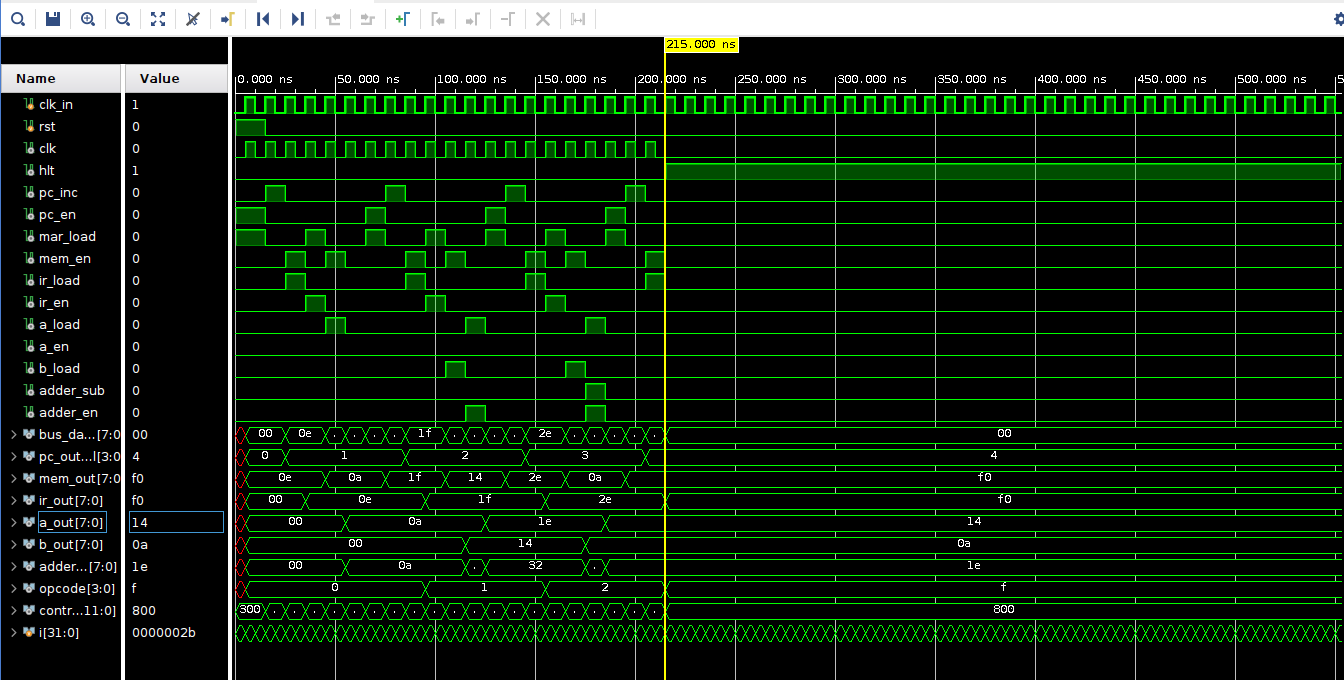
After about 215ns, our final result was available in a_out = 0x14
Translating code to real world
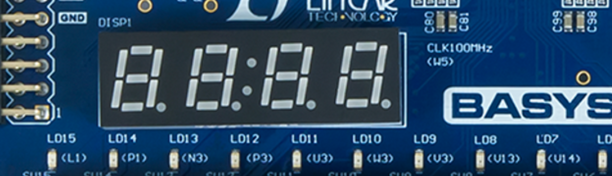
In order to see our FPGA perform the instructions, we will be taking help of the 7-segment display to see the ouput of our instructions.
To achieve this, we would need multiple modules.
- Binary to BCD Conversion : The 8-bit result (0-255) needs to be converted into three 4-bit Binary Coded Decimal (BCD) digits representing hundreds, tens, and ones.
- BCD to 7-Segment Encoding : Each BCD digit needs to be translated into the 7 signals (active-low for Basys 3 common anode display) required to light up the segments (a-g) for that digit.
- Display Multiplexing : The Basys 3 has 4 digits sharing the segment lines. We need to rapidly cycle through enabling each digit’s anode and driving the corresponding segment pattern. This requires a slower clock for the cycling (refresh rate) and logic to select the correct digit and its pattern at the right time.
1. binary_to_bcd.v
This module converts an 8-bit binary number into three 4-bit BCD digits using the “Double Dabble” (Shift-and-Add-3) algorithm. This is purely combinational.
// Module to convert 8-bit binary to 3-digit BCD
// Uses the Double Dabble (Shift-and-Add-3) algorithm

module binary_to_bcd (
    input  [7:0] bin_in,        // 8-bit binary input (Value: 0 to 255)

    output [3:0] bcd_hundreds,  // BCD digit for 100s place
    output [3:0] bcd_tens,      // BCD digit for 10s place
    output [3:0] bcd_ones       // BCD digit for 1s place
);

    // Internal register for the Double Dabble process.
    // Size: 3 * 4 bits (BCD) + 8 bits (Binary) = 20 bits.
    // Layout: [ Hundreds | Tens | Ones | Original Binary ]
    reg [19:0] dabble_reg;
    integer i; // Loop counter for shifts

    // Combinational logic: Recalculates whenever bin_in changes.
    always @(bin_in) begin
        // Step 1: Initialize the register.
        // Place the binary input in the lower 8 bits, BCD digits are initially 0.
        dabble_reg = {12'b0, bin_in};

        // Step 2: Perform 8 iterations (one for each bit of the input).
        for (i = 0; i < 8; i = i + 1) begin
            // Step 2a: Check each BCD digit *before* shifting.
            // If a digit is 5 or greater, add 3 to it.
            // Check Hundreds Digit (bits 19:16)
            if (dabble_reg[19:16] >= 4'd5) begin
                dabble_reg[19:16] = dabble_reg[19:16] + 4'd3;
            end
            // Check Tens Digit (bits 15:12)
            if (dabble_reg[15:12] >= 4'd5) begin
                dabble_reg[15:12] = dabble_reg[15:12] + 4'd3;
            end
            // Check Ones Digit (bits 11:8)
            if (dabble_reg[11:8] >= 4'd5) begin
                dabble_reg[11:8] = dabble_reg[11:8] + 4'd3;
            end

            // Step 2b: Shift the entire register left by 1 bit.
            dabble_reg = dabble_reg << 1;
        end
    end

    // Step 3: Assign the final BCD digits to the output ports.
    // The BCD digits are now in the upper 12 bits of the dabble_reg.
    assign bcd_hundreds = dabble_reg[19:16];
    assign bcd_tens     = dabble_reg[15:12];
    assign bcd_ones     = dabble_reg[11:8];

endmodule
2. bcd_to_7seg.v
This module takes a 4-bit BCD digit and outputs the 7 segment patterns. Crucially, it’s designed for the Basys 3’s common anode display, meaning segments are active LOW (0 turns ON).
// Description: Converts a 4-bit BCD digit (0-9) into 7-segment display
//              cathode patterns.
// Target:      Basys 3 (Common Anode Display -> Active-LOW Cathodes)

module bcd_to_7seg (
    input  [3:0] bcd_in,    // 4-bit BCD input (Value: 0 to 9)
    output [6:0] segments   // 7-segment cathode outputs {g,f,e,d,c,b,a} - Active LOW (0=ON)
                            // segments[0] = Segment A (Top)
                            // segments[1] = Segment B (Top-Right)
                            // segments[2] = Segment C (Bottom-Right)
                            // segments[3] = Segment D (Bottom)
                            // segments[4] = Segment E (Bottom-Left)
                            // segments[5] = Segment F (Top-Left)
                            // segments[6] = Segment G (Middle)
);

    reg [6:0] seg_out_reg; // Internal register for segment patterns

    // Combinational logic: Update segments whenever bcd_in changes.
    always @(bcd_in) begin
        case(bcd_in)
            // BCD -> segments {g,f,e,d,c,b,a} (Active LOW: 0=ON, 1=OFF)
            4'd0: seg_out_reg = 7'b1000000; // "0" (gfedcba = 1000000)
            4'd1: seg_out_reg = 7'b1111001; // "1" (gfedcba = 1111001)
            4'd2: seg_out_reg = 7'b0100100; // "2" (gfedcba = 0100100)
            4'd3: seg_out_reg = 7'b0110000; // "3" (gfedcba = 0110000)
            4'd4: seg_out_reg = 7'b0011001; // "4" (gfedcba = 0011001)
            4'd5: seg_out_reg = 7'b0010010; // "5" (gfedcba = 0010010)
            4'd6: seg_out_reg = 7'b0000010; // "6" (gfedcba = 0000010)
            4'd7: seg_out_reg = 7'b1111000; // "7" (gfedcba = 1111000)
            4'd8: seg_out_reg = 7'b0000000; // "8" (gfedcba = 0000000)
            4'd9: seg_out_reg = 7'b0010000; // "9" (gfedcba = 0010000)

            // For invalid BCD inputs (10-15), display blank (all segments OFF).
            default: seg_out_reg = 7'b1111111; // Blank
        endcase
    end

    // Assign the internal register to the output port.
    assign segments = seg_out_reg;

endmodule
3. seven_segment_controller.v
This is the core display driver. It takes the BCD digits, uses a slower clock derived from the main clock to cycle through the digits, enables the correct anode, and uses the bcd_to_7seg module to drive the segments. It also includes an enable input, which we will connect to the CPU’s hlt signal.
module seven_segment_controller (
    input         clk,       // System clock input (e.g., 100MHz)
    input         reset,     // System reset input (active high)
    input         enable,    // Display enable input (e.g., from CPU halt signal)

    // BCD digits from the binary_to_bcd converter
    input [3:0]   bcd_h,     // Hundreds digit
    input [3:0]   bcd_t,     // Tens digit
    input [3:0]   bcd_o,     // Ones digit

    // Outputs to the Basys 3 7-Segment Display Pins
    output reg [6:0] seg_out,  // Segment cathode outputs {g,f,e,d,c,b,a} (Active LOW)
    output reg [3:0] an_out    // Anode selector outputs {AN3,AN2,AN1,AN0} (Active LOW)
);

    // --- Parameters ---
    // Clock divider setup for display refresh rate
    // Target refresh rate per digit > 60Hz to avoid flicker.
    // With 100MHz clock:
    // 18 bits -> 2^18 / 100MHz = 2.62ms per digit -> ~95 Hz refresh per 4 digits.
    // 19 bits -> 5.24ms -> ~47 Hz refresh. Might flicker slightly.
    // 20 bits -> 10.48ms -> ~24 Hz refresh. Will likely flicker.
    // Let's use 18 bits for a faster refresh (~380 Hz per digit).
    localparam REFRESH_COUNTER_BITS = 18;

    // Define which digit selection value corresponds to which anode
    localparam ANODE_SEL_ONES      = 2'b00; // Rightmost digit (AN0)
    localparam ANODE_SEL_TENS      = 2'b01; // Digit AN1
    localparam ANODE_SEL_HUNDREDS  = 2'b10; // Digit AN2
    localparam ANODE_SEL_UNUSED    = 2'b11; // Leftmost digit (AN3) - currently unused/blank

    // --- Internal Signals ---
    reg [REFRESH_COUNTER_BITS-1:0] refresh_counter; // Counter for multiplexing
    wire [1:0] digit_select;      // Selects which digit (0-3) is currently active

    reg [3:0] current_bcd;        // BCD value for the currently selected digit
    wire [6:0] current_segments;  // Segment pattern for the current BCD value

    // --- Clock Divider for Refresh Rate ---
    // Free-running counter based on the system clock
    always @(posedge clk or posedge reset) begin
        if (reset) begin
            refresh_counter <= 0;
        end else begin
            refresh_counter <= refresh_counter + 1;
        end
    end

    // Use the top bits of the counter to select the active digit (00, 01, 10, 11)
    assign digit_select = refresh_counter[REFRESH_COUNTER_BITS-1 : REFRESH_COUNTER_BITS-2];

    // --- BCD Digit Multiplexer ---
    // Selects the appropriate BCD input based on the active digit
    always @(*) begin
        case (digit_select)
            ANODE_SEL_ONES:     current_bcd = bcd_o;        // AN0 -> Ones digit
            ANODE_SEL_TENS:     current_bcd = bcd_t;        // AN1 -> Tens digit
            ANODE_SEL_HUNDREDS: current_bcd = bcd_h;        // AN2 -> Hundreds digit
            ANODE_SEL_UNUSED:   current_bcd = 4'b1111;      // AN3 -> Display Blank (using default in BCD decoder)
            default:            current_bcd = 4'b1111;      // Default: Blank
        endcase
    end

    // --- Instantiate BCD to 7-Segment Decoder ---
    // Connect the currently selected BCD digit to the decoder
    bcd_to_7seg bcd_decoder (
        .bcd_in   (current_bcd),
        .segments (current_segments) // Gets the Active-LOW segment pattern
    );

    // --- Output Drive Logic ---
    // Drives the anode and segment outputs based on selection and enable signal
    always @(*) begin
        if (enable) begin
            // Display is enabled - drive segments and selected anode

            // Drive segments based on the decoder output (Active LOW)
            seg_out = current_segments;

            // Activate the selected Anode (Active LOW)
            // Only one anode is LOW at a time.
            case (digit_select)
                ANODE_SEL_ONES:     an_out = 4'b1110; // AN0 LOW, others HIGH
                ANODE_SEL_TENS:     an_out = 4'b1101; // AN1 LOW, others HIGH
                ANODE_SEL_HUNDREDS: an_out = 4'b1011; // AN2 LOW, others HIGH
                ANODE_SEL_UNUSED:   an_out = 4'b0111; // AN3 LOW, others HIGH (if displaying blank)
                                     // If truly unused, set to 4'b1111 here.
                                     // Let's drive it but show blank via current_bcd.
                default:            an_out = 4'b1111; // All anodes HIGH (OFF)
            endcase

        end else begin
            // Display is disabled - turn off all segments and anodes
            an_out = 4'b1111;      // All anodes HIGH (OFF)
            seg_out = 7'b1111111; // All segments HIGH (Segments OFF)
        end
    end

endmodule
4. Integrating in top module
Modify your sap1_cpu_top to include the display logic and add the necessary output ports.
// SAP-1 CPU Top-Level Module with 7-Segment Display Output

module sap1_cpu_top (
    input         clk_in,     // Clock input (Connect to Basys 3 100MHz oscillator, e.g., W5)
    input         rst,        // Reset input (Connect to a button or reset circuit)
    output        hlt_out,    // Output the halt signal status (e.g., to an LED)

    // Outputs for the 7-Segment Display
    output [6:0]  seg_out,    // Segment cathodes (Active LOW)
    output [3:0]  an_out      // Anode selectors (Active HIGH)
);

    // --- Internal Signal Declarations ---

    // Clocks and Reset (as before)
    wire clk;       // Gated clock used by most components
    wire hlt;       // Internal halt signal from controller

    // Control Signals (as before)
    wire pc_inc;
    wire pc_en;
    wire mar_load;
    wire mem_en;
    wire ir_load;
    wire ir_en;
    wire a_load;
    wire a_en;
    wire b_load;
    wire adder_sub;
    wire adder_en;
    wire [11:0] control_word;

    // Data Paths & Intermediate Signals (as before)
    wire [7:0] bus_data;
    wire [3:0] pc_out_internal;
    wire [7:0] mem_out;
    wire [7:0] ir_out;
    wire [7:0] a_out; // <<< This holds the final result
    wire [7:0] b_out;
    wire [7:0] adder_out;
    wire [3:0] opcode;

    // --- Instantiate Clock Module --- (as before)
    clock u_clock (
        .clk_100mhz (clk_in),
        .hlt        (hlt),
        .clk_out    (clk)
    );

    // --- Instantiate CPU Components --- (as before)
    pc u_pc (.clk(clk), .rst(rst), .inc(pc_inc), .out(pc_out_internal));
    memory u_memory (.clk(clk), .rst(rst), .load(mar_load), .bus(bus_data), .out(mem_out));
    reg_a u_reg_a (.clk(clk), .rst(rst), .load(a_load), .bus(bus_data), .out(a_out));
    reg_b u_reg_b (.clk(clk), .rst(rst), .load(b_load), .bus(bus_data), .out(b_out));
    adder u_adder (.in_a(a_out), .in_b(b_out), .sub(adder_sub), .result(adder_out)); // Check '.sub' vs '.subt' if you used a different name
    ir u_ir (.clk(clk), .rst(rst), .load(ir_load), .bus(bus_data), .out(ir_out));

    // --- Instantiate Controller --- (as before)
    assign opcode = ir_out[7:4];
    controller u_controller (.clk(clk), .rst(rst), .opcode(opcode), .out(control_word));

    // --- Deconstruct Control Word --- (as before)
    assign hlt       = control_word[11];
    assign pc_inc    = control_word[10];
    assign pc_en     = control_word[9];
    assign mar_load  = control_word[8];
    assign mem_en    = control_word[7];
    assign ir_load   = control_word[6];
    assign ir_en     = control_word[5];
    assign a_load    = control_word[4];
    assign a_en      = control_word[3];
    assign b_load    = control_word[2];
    assign adder_sub = control_word[1];
    assign adder_en  = control_word[0];

    // --- Instantiate Bus Multiplexer --- (as before)
    bus_mux u_bus_mux (
        .adder_out(adder_out), .a_out(a_out), .ir_out(ir_out), .mem_out(mem_out), .pc_out(pc_out_internal),
        .adder_en(adder_en), .a_en(a_en), .ir_en(ir_en), .mem_en(mem_en), .pc_en(pc_en),
        .bus_data(bus_data)
    );

    // --- Instantiate Display Logic ---

    // 1. Convert final result (a_out) to BCD
    wire [3:0] bcd_h_w, bcd_t_w, bcd_o_w;
    binary_to_bcd u_bin_to_bcd (
        .bin_in       (a_out), // Input is the result from Register A
        .bcd_hundreds (bcd_h_w),
        .bcd_tens     (bcd_t_w),
        .bcd_ones     (bcd_o_w)
    );

    // 2. Instantiate the 7-Segment Controller
    seven_segment_controller u_display_controller (
        .clk      (clk_in), // Use the fast main clock for the controller's internal divider
        .reset    (rst),
        .enable   (hlt),    // Enable display only when CPU is halted
        .bcd_h    (bcd_h_w),
        .bcd_t    (bcd_t_w),
        .bcd_o    (bcd_o_w),
        .seg      (seg_out), // Connect to top-level output
        .an       (an_out)   // Connect to top-level output
    );

    // --- Assign Top-Level Outputs ---
    assign hlt_out = hlt;

endmodule
Loading it onto our FPGA
We will be using the Basys3 (Xilinx Artix-7 FPGA: XC7A35T-1CPG236C) board for this project.
Basys3 board schematic
Also refer to basys3-master.xdc.
Transclude of basys3-master.xdc
The
.xdc file basically maps inputs and outputs from our verilog code to physical ports on the board.
8-bit-cpu xdc file
This is the .xdc file we need for our CPU, add it as a constraint source in our vivado project.
## Basys 3 Constraints File for SAP-1 CPU Project
## Target Device: Xilinx Artix-7 XC7A35T-1CPG236C

#------------------------------------------------------------------------------
# Clock Signal
#------------------------------------------------------------------------------
# Connects to the 100MHz oscillator on the Basys 3 board (Pin W5)
set_property -dict { PACKAGE_PIN W5   IOSTANDARD LVCMOS33 } [get_ports clk_in]
# Define the clock period (10ns for 100MHz) for timing analysis
create_clock -add -name sys_clk_pin -period 10.00 -waveform {0 5} [get_ports clk_in]

#------------------------------------------------------------------------------
# Reset Button
#------------------------------------------------------------------------------
# Connects to the Center Push Button (BTNC - Pin U18)
set_property -dict { PACKAGE_PIN U18 IOSTANDARD LVCMOS33 } [get_ports rst]

#------------------------------------------------------------------------------
# Halt Status LED
#------------------------------------------------------------------------------
# Connects to LED LD0 (Pin U16) to indicate CPU halt status
set_property -dict { PACKAGE_PIN U16 IOSTANDARD LVCMOS33 } [get_ports hlt_out]

#------------------------------------------------------------------------------
# 7-Segment Display
#------------------------------------------------------------------------------
## Segment Cathodes (Active LOW)
# Maps seg_out[6:0] to segments g,f,e,d,c,b,a respectively
set_property -dict { PACKAGE_PIN W7   IOSTANDARD LVCMOS33 } [get_ports {seg_out[0]}] ;# Segment A
set_property -dict { PACKAGE_PIN W6   IOSTANDARD LVCMOS33 } [get_ports {seg_out[1]}] ;# Segment B
set_property -dict { PACKAGE_PIN U8   IOSTANDARD LVCMOS33 } [get_ports {seg_out[2]}] ;# Segment C
set_property -dict { PACKAGE_PIN V8   IOSTANDARD LVCMOS33 } [get_ports {seg_out[3]}] ;# Segment D
set_property -dict { PACKAGE_PIN U5   IOSTANDARD LVCMOS33 } [get_ports {seg_out[4]}] ;# Segment E
set_property -dict { PACKAGE_PIN V5   IOSTANDARD LVCMOS33 } [get_ports {seg_out[5]}] ;# Segment F
set_property -dict { PACKAGE_PIN U7   IOSTANDARD LVCMOS33 } [get_ports {seg_out[6]}] ;# Segment G

## Anode Selectors (Active HIGH)
# Maps an_out[3:0] to AN3, AN2, AN1, AN0 respectively (Left to Right)
set_property -dict { PACKAGE_PIN U2   IOSTANDARD LVCMOS33 } [get_ports {an_out[0]}] ;# Anode 0 (Rightmost)
set_property -dict { PACKAGE_PIN U4   IOSTANDARD LVCMOS33 } [get_ports {an_out[1]}] ;# Anode 1
set_property -dict { PACKAGE_PIN V4   IOSTANDARD LVCMOS33 } [get_ports {an_out[2]}] ;# Anode 2
set_property -dict { PACKAGE_PIN W4   IOSTANDARD LVCMOS33 } [get_ports {an_out[3]}] ;# Anode 3 (Leftmost)

#------------------------------------------------------------------------------
# General Configuration Settings (Recommended for all Basys 3 designs)
#------------------------------------------------------------------------------
set_property CONFIG_VOLTAGE 3.3 [current_design]
set_property CFGBVS VCCO [current_design]

#------------------------------------------------------------------------------
# SPI Configuration Settings (for programming via QSPI Flash)
#------------------------------------------------------------------------------
set_property BITSTREAM.GENERAL.COMPRESS TRUE [current_design]
set_property BITSTREAM.CONFIG.CONFIGRATE 33 [current_design]
set_property CONFIG_MODE SPIx4 [current_design]
Upgrading a bit
ALU
Here’s the new instruction set:
| Mnemonic | Opcode (Hex) | Syntax | Machine Code | Function |
|---|---|---|---|---|
| LDA | 0 | LDA addr | 0addr | Loads value from memory address into Register A |
| ADD | 1 | ADD addr | 1addr | Adds value from memory address to Register A |
| SUB | 2 | SUB addr | 2addr | Subtracts value from memory address from Register A |
| AND | 5 | AND addr | 5addr | Performs bitwise AND between memory value and Register A |
| OR | 6 | OR addr | 6addr | Performs bitwise OR between memory value and Register A |
| XOR | 7 | XOR addr | 7addr | Performs bitwise XOR between memory value and Register A |
| NOTA | 8 | NOTA addr | 8addr | Performs bitwise NOT on Register A (addr ignored) |
| HLT | F | HLT | F0 | Halts the CPU |
Stepping through instructions one by one
Here are all the final files
CPU
Transclude of sap_1_cpu_top.v
Transclude of clock.v
Transclude of memory.v
Transclude of ir.v
Transclude of pc.v
Transclude of alu.v
Transclude of controller.v
Transclude of bus_mux.v
Transclude of reg_a.v
Transclude of reg_b.v
7-segment
Transclude of binary_to_bcd.v
Transclude of bcd_to_7seg.v
Transclude of seven_segment_controller.v
Testbench and constraint
Transclude of basys3.xdc
Transclude of top_tb.v